SK hynix expands US engineering team for custom Nvidia memory
Packaging specialists will coordinate custom HBM integration while backing the chipmaker's $4 billion advanced packaging fab in Indiana.
SK hynix decided Nov. 9, 2026, to expand its American technical workforce, deploying packaging engineers to deepen custom high-bandwidth memory integration with Nvidia and North American cloud providers.
The South Korean chipmaker held 58% of global high-bandwidth memory revenue in the first quarter of 2026. High-bandwidth memory stacks dynamic random-access memory vertically to speed data transfers inside artificial intelligence accelerators.
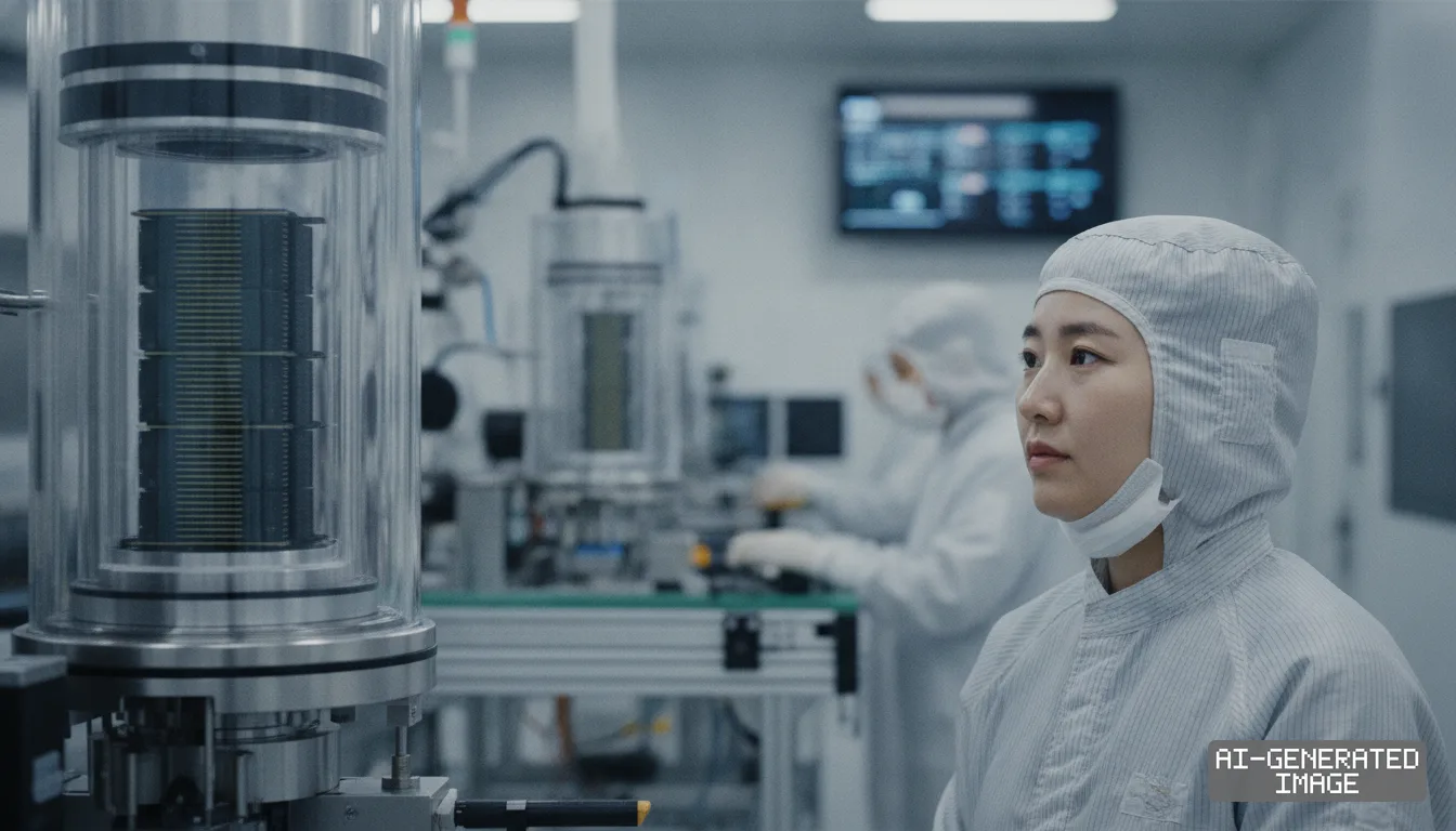
The engineering deployment supports an advanced packaging fabrication facility in West Lafayette, Indiana, where total investment exceeds $4 billion. The 133-acre campus will house cleanrooms and an advanced packaging testbed.
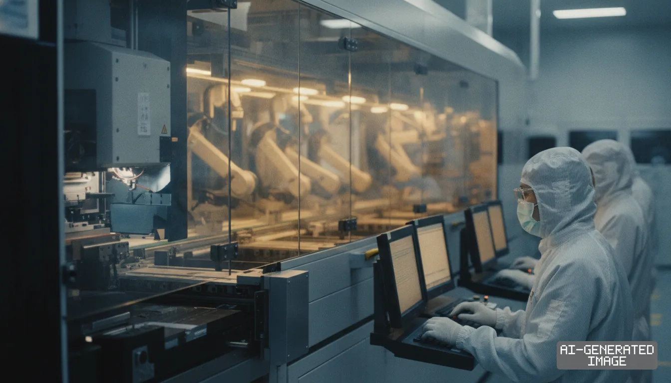
The expansion shifts the regional footprint from commercial sales toward collaborative technical development. Operating personnel will work alongside client architects in Silicon Valley to align memory physical layers with processor packaging.
Memory customization focuses on the base die — the bottom logic chip that coordinates data transfer between the memory stack and the processor. Customer specifications require unique logic dies to minimize electrical latency.
Nvidia takes more than half of high-bandwidth memory shipments from SK hynix. The accelerator designer requires custom base dies to integrate directly with its graphics processors and server clusters.
Nvidia also asked memory suppliers to standardize custom base dies on Taiwan Semiconductor Manufacturing Co.'s 3-nanometer logic node. The shared manufacturing process ensures uniform electrical performance across memory modules.
A multi-year technology partnership signed June 8, 2026, binds SK hynix and Nvidia to co-develop memory for AI factories. The agreement targets accelerator architectures designed for automated computing centers.
The technical deployment builds on executive appointments announced Oct. 30, which took effect Nov. 1. SK hynix created a president-level Americas division to oversee regional manufacturing, client engagements and technical operations.
Ahn Hyun, previously chief development officer heading high-bandwidth memory and custom module programs, assumed leadership of the Americas division. Ahn directs local engineering teams from California.
Cha Seon-yong succeeded Ahn as chief development officer while retaining management of the Future Technology Research Institute. The dual role links fundamental materials research with production roadmaps.
Yoon Poong-young took office as president of the Corporate Center to supervise capital spending and global operations. Yoon manages strategic resource allocation across overseas manufacturing facilities.
The Indiana facility will process silicon wafers fabricated at front-end semiconductor fabs in South Korea. Specialized cargo networks will transport processed wafers across the Pacific for domestic finishing.
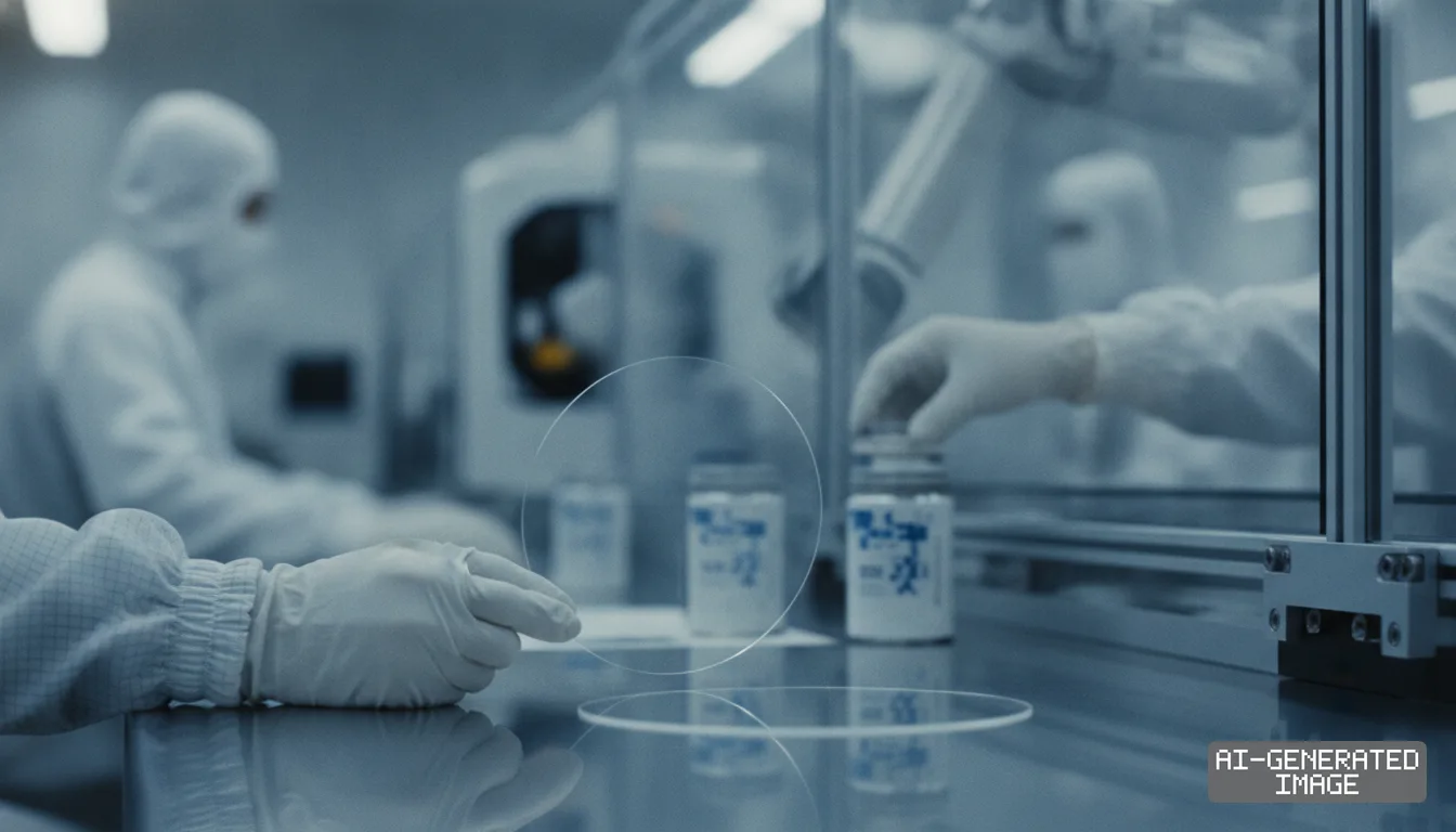
Technicians in Indiana will execute through-silicon via bonding, wafer dicing and liquid resin encapsulation. The site will test completed stacks before delivering finished components to American data centers.
The packaging plant will employ approximately 1,000 personnel once production reaches scale. Company projections indicate the facility and related supply chain networks will support 7,000 direct and indirect jobs.
The U.S. Department of Commerce awarded the Indiana project preliminary terms for up to $450 million in direct funding under the CHIPS and Science Act. The preliminary agreement also includes $500 million in loans.
SK hynix also applied for the Advanced Manufacturing Investment Tax Credit through the U.S. Department of the Treasury. The program provides credits covering up to 25% of qualified capital expenditures on domestic semiconductor facilities.
An academic partnership with Purdue University establishes a joint research program on the West Lafayette campus. The initiative trains specialized packaging operators and evaluates experimental bonding equipment.
SK hynix has not published a regulatory filing specifying the exact headcount target, operating budget or job band breakdown for the Silicon Valley engineering expansion.
Follow-up personnel appointments and departmental restructuring for the American team take effect Dec. 3, 2026. Cleanroom construction at the Indiana packaging site concludes in October 2028 ahead of mass production scheduled for late 2029.
Impact map
How this development propagates across the region and out to global buyers.
| Event | Korea | China | Japan | Global impact |
|---|---|---|---|---|
| U.S. engineering expansion | SK hynix binds custom HBM4E base dies to Nvidia architectures while keeping DRAM wafer fabrication domestic | Domestic memory makers CXMT and YMTC remain restricted from advanced packaging equipment and custom base die supply chains | Semiconductor materials vendors Tokyo Ohka Kogyo and Resonac secure packaging chemical supply lines for U.S. plants | Hyperscalers gain dedicated co-design channels that reduce AI accelerator memory latency and thermal loads |
In this story
Track every Subsidies development →
Related briefings
- SK hynix names lead HBM developer to head new Americas unit Also on Nvidia, SK hynix, Subsidies
- GlobalFoundries signs $2 billion TSMC chip interposer deal Also on Nvidia, SK hynix, Subsidies
- GlobalFoundries signs $2B TSMC packaging deal for AI chips Also on Nvidia, SK hynix, Subsidies
- TSMC widens CoWoS supply chain with $2 billion US interposer deal Also on Nvidia, SK hynix, Subsidies
Sources
Primary documents
Reporting
Confidence: high — how we grade this
The documents behind this briefing are linked above. East Asia Brief produces its English text with AI assistance under human editorial review, and does not translate or republish other outlets' articles. See our methodology and AI policy. Spotted an error? Tell us.
The Morning Brief
What changed in Korean, Chinese and Japanese industry overnight — and what it means for your supply chain. One email, weekday mornings, US time. Free.
The Morning Brief is in preparation. Leave your address and we will write to you once — when the first issue is ready. Nothing before that.