SK hynix begins supplier talks for 30% cooler iHBM AI memory
The South Korean chipmaker aims to embed silicon cooling elements into HBM5 stacks, curbing heat bottlenecks in high-density AI accelerators.
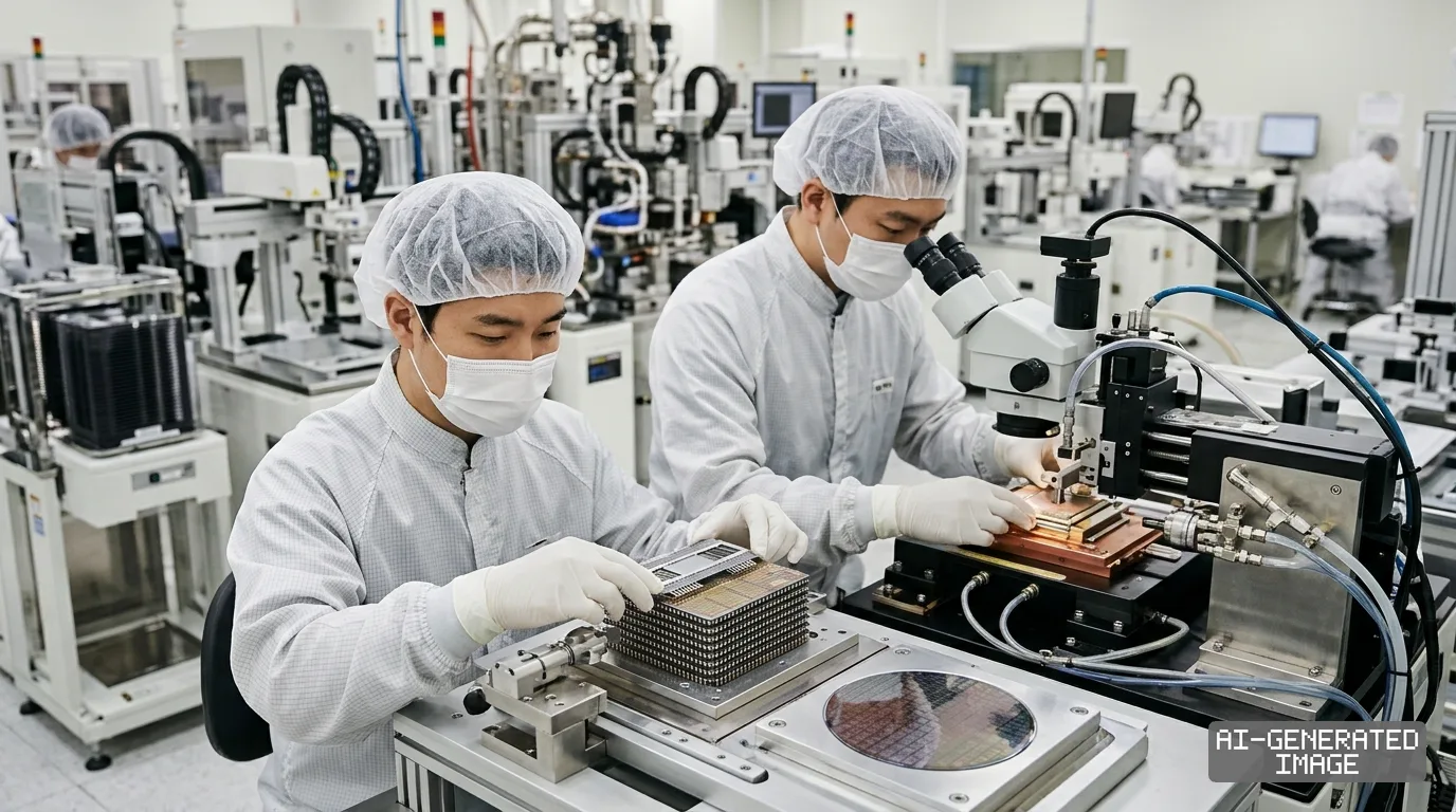
SK hynix opened technical talks with semiconductor equipment and materials suppliers on Oct. 21 to prepare commercial manufacturing for iHBM, its cooling-integrated architecture aimed at high-bandwidth memory.
The initiative moves proprietary thermal technology toward commercial production lines. SK hynix accounts for more than half of global high-bandwidth memory shipments used in artificial intelligence accelerators.
The memory maker first detailed the architecture on May 26, reporting that iHBM cuts thermal resistance by more than 30% compared to standard memory stacks. That reduction tackles a major physical bottleneck in data centers.
Thermal management has emerged as a limiting factor for advanced computing clusters. As memory dies stack higher to feed graphics processors, heat builds up inside server chassis.
SK hynix stated at the Hot Chips conference that cumulative thermal burdens run 2.2 times higher across recent memory generations. Memory stacks face strict mechanical ceilings inside multi-chip modules.
Conventional packages transfer heat indirectly through core dies to external plates. That approach slows heat dissipation when computing workloads surge to peak capacity.
The iHBM design places Integrated Cooling Elements directly into the die-to-die physical layer. That interface forms the primary hardware channel connecting the memory base die to the processor.
These cooling elements consist of silicon-based materials that conduct heat without carrying electrical current. The structure creates an immediate evacuation path away from hot spots.
Direct dissipation prevents thermal throttling during sustained artificial intelligence training workloads. It also helps preserve switching speeds across densely clustered memory cells.
The architecture relies on mass reflow molded underfill, an established bonding method. Liquid epoxy fills spaces between stacked chips before hardening into a protective shield.
Using wafer-level packaging allows SK hynix to build iHBM without redesigning fabrication lines from scratch. It also preserves compatibility with existing system-in-package standards.
System compatibility lets accelerator designers adopt new thermal options without modifying substrate footprints. Major chip buyers demand drop-in packaging solutions to protect hardware schedules.
Nvidia requires 288 gigabytes of memory on its Vera Rubin platform, making module heat a critical engineering threshold. Memory thermal failure forces accelerators to throttle processing cycles.
SK hynix collaborates with Taiwan Semiconductor Manufacturing Co. on packaging integration. TSMC manufactures the underlying logic bases and assembles memory cubes using chip-on-wafer-on-substrate technology.
The commercial roadmap assigns iHBM integration to eighth-generation memory, designated HBM5. The company plans to deploy the architecture after concluding current production cycles for HBM4 and HBM4E.
Industry deployment schedules target initial HBM5 volume manufacturing around 2029. Memory suppliers must validate tooling years ahead to align wafer lines with foundry cycles.
Domestic and overseas equipment makers must build custom inspection tools for the cooling blocks. Materials suppliers must also deliver certified batches of thermal silicon compounds.
The company has not published supplier contracts, pilot-line dates or capital expenditure figures in regulatory filings. Neither SK hynix nor the Korea Exchange released official disclosures on Oct. 21.
SK hynix plans to continue technical qualification tests with foundry partners before locking tooling specifications for volume assembly.
Impact map
How this development propagates across the region and out to global buyers.
| Event | Korea | China | Japan | Global impact |
|---|---|---|---|---|
| iHBM supplier talks | SK hynix qualifies domestic packaging tool vendors for HBM5 lines | Hyperscale data centers face widening thermal efficiency gap | Materials firms receive preliminary specs for non-conductive silicon | AI server clusters gain 30% thermal resistance reduction in memory |
In this story
Related briefings
- GlobalFoundries signs $2B TSMC packaging deal for AI chips Also on TSMC, Nvidia, SK hynix
- SK hynix and Samsung push 16-layer HBM4 as Nvidia caps Rubin at 12 dies Also on TSMC, Nvidia, SK hynix
- Samsung revamps HBM thermal packaging to challenge TSMC supply lead Also on TSMC, Nvidia, SK hynix
- Micron taps TSMC for custom HBM4E memory, taking on SK hynix Also on TSMC, Nvidia, SK hynix
Sources
Reporting
Confidence: medium — how we grade this
The documents behind this briefing are linked above. East Asia Brief produces its English text with AI assistance under human editorial review, and does not translate or republish other outlets' articles. See our methodology and AI policy. Spotted an error? Tell us.
The Morning Brief
What changed in Korean, Chinese and Japanese industry overnight — and what it means for your supply chain. One email, weekday mornings, US time. Free.
The Morning Brief is in preparation. Leave your address and we will write to you once — when the first issue is ready. Nothing before that.