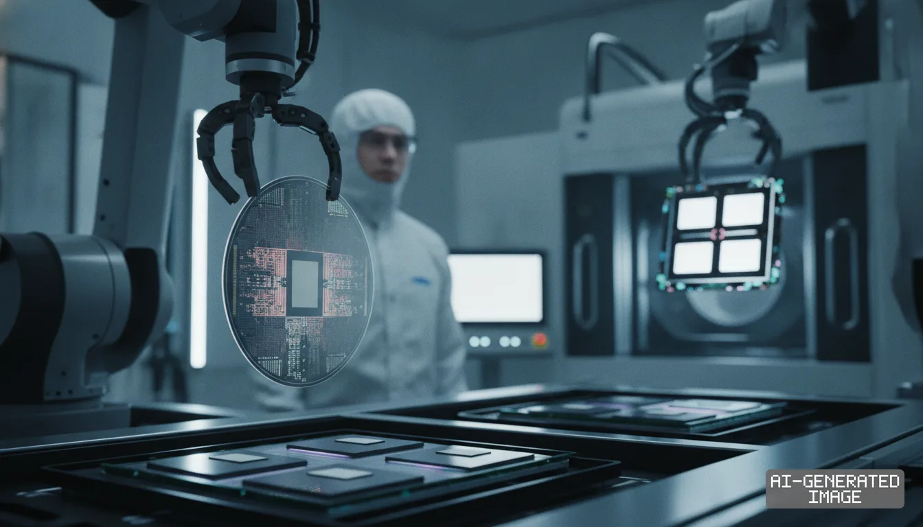
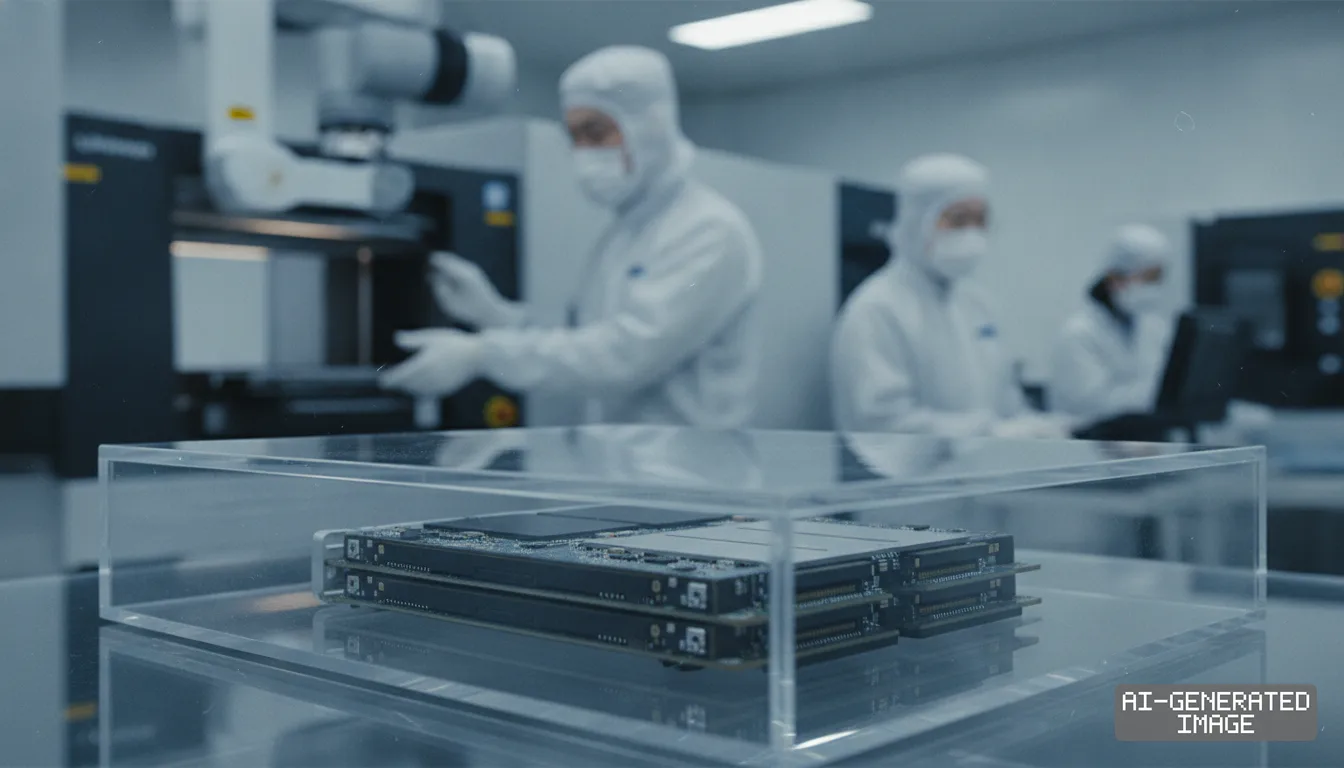
Samsung says HBM will take 30% of DRAM wafer capacity by 2027
The shift crowds out standard DDR5 output across shared lines, while research firm TrendForce projects average selling prices for stacked memory will surge 121%.
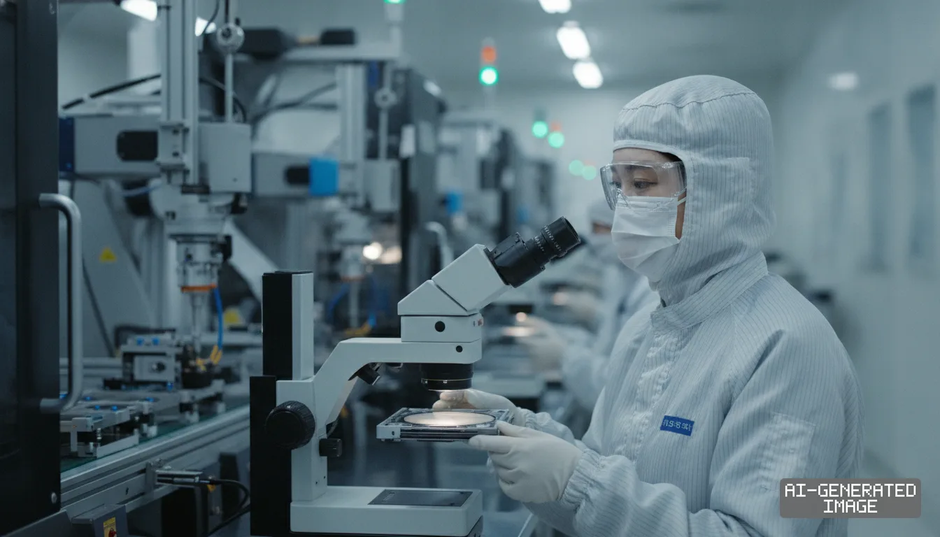
Samsung Electronics executive Kim Tae-woo said Sept. 30 that high-bandwidth memory will absorb nearly 30% of global DRAM wafer capacity next year, directly constraining manufacturing lines available for standard memory chips.
The South Korean company holds roughly 40% of worldwide dynamic random-access memory supply. Its cleanrooms fabricate advanced stacked artificial intelligence modules on the same production lines that produce conventional memory for personal computers.
High-bandwidth memory consumed 18% of global DRAM wafer starts at the end of 2025. That share climbed to 22% during 2026 and will reach 30% by late 2027, according to research firm TrendForce.
The heavy wafer input delivers an asymmetrical bit output. High-bandwidth stacks will yield roughly 13% of total memory bit supply in 2027, after generating 8% in 2025 and 9% in 2026.
A single high-bandwidth memory die consumes roughly three times the physical wafer area of a standard DDR5 computing die. That surface penalty reduces the count of functional memory dies produced per processed wafer.
Vertical assembly compounds the silicon overhead. Packaging eight or 12 dies using through-silicon vias — microscopic vertical copper pathways etched through silicon — causes yield loss where a single flawed layer discards an entire multi-die stack.
Samsung will expand its monthly high-bandwidth memory wafer starts by nearly 40% next year to address orders. Processing volume will grow from 180,000 wafers monthly in 2026 to roughly 250,000 wafers monthly during 2027.
Advanced HBM4 packages will make up 80% of Samsung's dedicated memory shipments next year. The newer architecture relies on logic base dies, adding complex manufacturing steps that occupy cleanroom capacity previously open to commodity memory.
The reallocation removes cleanroom capacity from standard dynamic random-access memory. Memory lines that produce dual in-line memory modules for corporate networks and desktop systems are losing tool time to artificial intelligence accelerators.
Mobile device manufacturers face immediate supply limits for low-power double data rate components. Suppliers have shifted front-end processing from smartphone lines toward artificial intelligence memory, keeping mobile memory unit production growth below 6% annually.
Handset brands have begun freezing device specifications to manage component availability. Leading smartphone producers are maintaining 12-gigabyte configurations rather than upgrading flagship handsets to 16 gigabytes because of reduced supply in mobile dynamic random-access memory.
Enterprise server operators face an identical squeeze on central processing memory. Next-generation server motherboards allocate more double data rate memory channels to host processors, requiring high-density 64-gigabyte and 128-gigabyte registered modules for each deployed graphics accelerator.
Shrinking line availability has accelerated memory price increases across commercial procurement contracts. TrendForce raised its 2027 price outlook Sept. 29, forecasting blended average selling prices for high-bandwidth memory will rise 121% from prior levels.
Commodity memory prices have climbed in response to the reduced factory capacity. Contract rates for 64-gigabyte DDR5 server modules rose from $380 in early 2025 to between $820 and $890 during the third quarter of 2026.
SK hynix and Micron Technology face the same factory capacity trade-offs across their operations. Together with Samsung, the three manufacturers supply roughly 90% of global dynamic random-access memory chips.
SK hynix has directed advanced equipment at its Icheon and Cheongju plants in South Korea toward multi-layer assembly. The company has pre-sold its high-bandwidth memory production volume through the upcoming operating year.
Micron has dedicated advanced fabrication equipment at its facility in Hiroshima, Japan, to multi-layer components. The company said at an industry conference that the silicon area penalty grows larger with each successive memory generation.
Server designers have evaluated architecture adjustments to control component expenses. Hardware developers are testing eight-layer stacks rather than 12-layer units to reduce physical wafer usage and protect processor production schedules.
Eight-layer configurations carry an economic trade-off for system builders. Because the cost of the underlying base die spreads over fewer gigabytes, eight-layer packages trade at a 10% to 20% price premium per gigabit over 12-layer stacks.
Cleanroom expansions from new greenfield semiconductor fabs will provide no production relief before late 2027. Tool installation and trial wafer cycles delay commercial output from newly constructed cleanrooms until the middle of 2028.
Enterprise buyers and memory fabricators begin annual 2027 contract pricing discussions in November. Those talks will determine how remaining wafer capacity divides between corporate server memory and accelerator stacks.
Samsung has not published the 30% wafer projection in a formal regulatory filing or investor relations release, and competitors SK hynix and Micron have not issued comparable company-level targets.
Global fabrication facilities operate at maximum equipment utilization as chipmakers finalize their manufacturing allocations for the coming year.
Impact map
How this development propagates across the region and out to global buyers.
| Event | Korea | China | Japan | Global impact |
|---|---|---|---|---|
| HBM wafer capacity surge | Samsung and SK hynix shift ~30% of DRAM wafers to HBM, cutting standard DDR5 lines | Domestic cloud and smartphone OEMs face reduced LPDDR5X supply and 12GB RAM caps | Micron Hiroshima ramps multi-layer HBM wafer allocation, tightening domestic DDR5 supply | AI server BOM up as HBM blended ASP rises 121% and DDR5 server modules top $820 |
In this story
- Companies
- Samsung Electronics
- Tickers
- 005930.KS
- Exposed
- SK hynixMicron Technology
- Policy
- Economic Security
- Impact
- Supply ChainPricingCapex
Track every Economic Security development →
Related briefings
- Nvidia locks up 37% of global HBM supply for AI accelerators Also on Micron Technology, SK hynix, Samsung Electronics
- DeepSeek cuts AI memory use 75%, rattling global chipmakers Also on Micron Technology, SK hynix, Samsung Electronics
- CXMT starts 5th-gen DRAM output, bypassing US tool controls Also on Micron Technology, SK hynix, Samsung Electronics
- CXMT beats SK hynix and Micron in DRAM margin at 87.59% gross rate Also on Micron Technology, SK hynix, Samsung Electronics
Sources
Reporting
Confidence: medium — how we grade this
The documents behind this briefing are linked above. East Asia Brief produces its English text with AI assistance under human editorial review, and does not translate or republish other outlets' articles. See our methodology and AI policy. Spotted an error? Tell us.
The Morning Brief
What changed in Korean, Chinese and Japanese industry overnight — and what it means for your supply chain. One email, weekday mornings, US time. Free.
The Morning Brief is in preparation. Leave your address and we will write to you once — when the first issue is ready. Nothing before that.