Samsung Electronics plans $18.7B Giheung fab to expand 2nm lines
The South Korean chipmaker is clearing research sites at its oldest semiconductor campus to accelerate advanced logic production for next-generation AI processors.
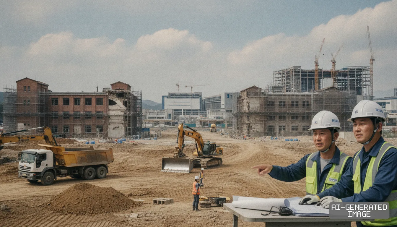
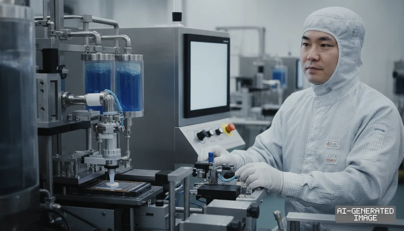
Samsung Electronics moved Nov. 4 to expand its contract chipmaking footprint, preparing brownfield land at its Giheung campus for an estimated $18.7 billion advanced foundry project.
The development repurposes industrial acreage at the company's oldest semiconductor campus in South Korea. The site previously housed the Samsung Advanced Institute of Technology research facility and the Corporate Development Institute.
Initial construction work is already underway under an affiliated engineering agreement. Samsung E&A disclosed a 407.1 billion won ($305 million) framework contract on Oct. 29, representing 4.51% of its 2025 revenue.
The regulatory filing covers civil framework construction for the Kairos complex, an industrial green utility building and an electrical substation. Samsung E&A scheduled structural handover for Dec. 31, 2028.
Industry estimates put the overall project cost at approximately 25 trillion won ($18.7 billion). That capital expenditure projection covers cleanroom infrastructure and extreme ultraviolet lithography systems from overseas suppliers.
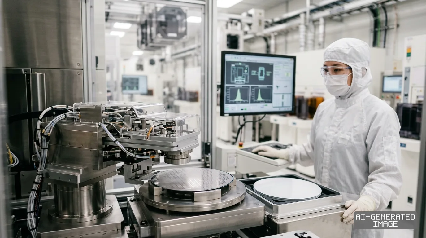
Samsung Electronics designed the facility to manufacture advanced logic chips using 2-nanometer and 4-nanometer production processes. Fab output will focus heavily on accelerating orders from global artificial intelligence customers.
A core manufacturing target for the Giheung lines is the base die for high-bandwidth memory. A base die — the foundational logic chip that routes signals beneath vertical stacks of dynamic random-access memory — governs thermal dissipation and interconnect speed.
Starting with sixth-generation memory known as HBM4, memory suppliers must fabricate base dies on advanced logic foundry nodes. Earlier memory designs relied on conventional DRAM production lines with wider circuitry.
The technological shift requires tighter integration between advanced packaging and front-end wafer fabrication. Samsung Electronics aims to offer customers a turnkey package combining memory fabrication, custom base logic and chiplet packaging.
By clearing existing research facilities in Giheung, Samsung Electronics bypasses multi-year delays in securing power lines and water permits. Greenfield industrial projects in South Korea typically require prolonged regulatory reviews.
The planned Yongin semiconductor mega-cluster faces years of utility grid installations before its first production lines can receive power. Giheung already maintains operational substations connected directly to national transmission networks.
Samsung Electronics previously delayed tool installations at its Pyeongtaek P4 production line and pushed out schedules in Taylor, Texas. The company adjusted its capital allocation to match actual fabless customer commitments.
Giheung provides immediate access to high-voltage power grids and industrial water networks. Reusing brownfield infrastructure reduces upfront civil preparation costs and compresses installation timelines.
Wafers fabricated at Giheung will route directly to advanced packaging facilities in Cheonan and Onyang. Short transit distances between domestic fabrication and packaging sites reduce turnaround times for high-bandwidth memory.
The initiative directly addresses market dominance held by Taiwan Semiconductor Manufacturing Co. TSMC commands more than 60% of worldwide foundry revenue and roughly 90% of advanced packaging capacity.
Samsung Electronics held less than 12% of the global contract chipmaking market last quarter. The foundry division has struggled to secure consistent volume commitments from major American fabless clients.
Nvidia purchases nearly all of its leading graphics processors and artificial intelligence accelerators from TSMC. Major American chip designers seek secondary manufacturing partners to mitigate supply concentration risks and temper fabrication costs.
Samsung E&A will book the construction proceeds across nine consecutive fiscal quarters. The engineering contractor reported 9.03 trillion won ($6.76 billion) in consolidated annual revenue for 2025.
The contractor amended its original agreement on Oct. 28 after contract adjustments surpassed Korea Exchange disclosure thresholds. Samsung Electronics will disburse construction payments in stages as site milestones are verified.
The project will also redirect domestic supply channels for semiconductor fabrication equipment. Domestic etching and deposition suppliers will compete directly against Japanese and American toolmakers for cleanroom orders.
Tokyo Electron and Canon supply coating, chemical processing and lithography systems to Samsung fabrication plants. Both Japanese equipment makers generate more than 15% of annual revenue from South Korean chipmakers.
South Korean toolmakers Wonik IPS and SEMES will target automated material handling and auxiliary cleanroom systems. Tool deliveries will follow structural building completion during the first half of 2029.
Trade rules continue to govern client access for advanced semiconductor fabrication nodes. Multilateral export controls restrict Chinese chip design firms from acquiring sub-14-nanometer foundry services without government licenses.
Because of these trade controls, Samsung Electronics must fill Kairos production capacity with orders from Western and domestic clients. The facility cannot rely on high-volume Chinese mobile or compute silicon.
The South Korean government supports semiconductor facility investments through corporate tax credits under the Act on Restriction of Special Taxation. Qualified investments receive tax deductions on eligible fabrication equipment spending.
The operational timeline for commercial wafer production depends on machinery delivery intervals. Extreme ultraviolet lithography systems carry delivery lead times exceeding 18 months from Dutch supplier ASML Holding.
The construction contract specifies structural completion by Dec. 31, 2028, according to the regulatory disclosure. Cleanroom installation and trial wafer runs will extend beyond that structural deadline.
Samsung Electronics has not published a corporate filing or official release confirming the 25 trillion won headline figure or operational timing for Project Kairos.
Impact map
How this development propagates across the region and out to global buyers.
| Event | Korea | China | Japan | Global impact |
|---|---|---|---|---|
| Giheung Kairos fab investment | Samsung E&A books 407.1 billion won, representing 4.51% of annual revenue | mainland fabless firms face export control bans on sub-14nm foundry access | Tokyo Electron and Canon position coating and lithography lines for 2028 deliveries | TSMC retains lead while Nvidia gains dual-sourcing leverage for HBM4 base dies |
| Giheung Kairos fab investment | Samsung E&A books 407.1 billion won, representing 4.51% of annual revenue | mainland fabless firms face export control bans on sub-14nm foundry access | Tokyo Electron and Canon position coating and lithography lines for 2028 deliveries | TSMC retains lead while Nvidia gains dual-sourcing leverage for HBM4 base dies |
In this story
- Companies
- Samsung ElectronicsSamsung E&A
- Tickers
- 005930.KS028050.KS
- Exposed
- Taiwan Semiconductor Manufacturing Co.Nvidia
- Policy
- Tax Credits
- Impact
- CapexSupply ChainOrder Book
Track every Tax Credits development →
Related briefings
- TSMC weighs Texas foundry campus to expand US chip capacity Also on Taiwan Semiconductor Manufacturing Co., Tax Credits, Nvidia
- TSMC Dismisses Terafab Rumors as Texas Factory Talks Surface Also on Taiwan Semiconductor Manufacturing Co., Tax Credits, Samsung Electronics
- TSMC plans new 3nm Tainan fab as AI accelerator demand surges Also on Taiwan Semiconductor Manufacturing Co., Nvidia, Samsung Electronics
- TSMC weighs Texas fab campus to broaden US foundry footprint Also on Taiwan Semiconductor Manufacturing Co., Nvidia, Samsung Electronics
Sources
Reporting
Confidence: medium — how we grade this
The documents behind this briefing are linked above. East Asia Brief produces its English text with AI assistance under human editorial review, and does not translate or republish other outlets' articles. See our methodology and AI policy. Spotted an error? Tell us.
The Morning Brief
What changed in Korean, Chinese and Japanese industry overnight — and what it means for your supply chain. One email, weekday mornings, US time. Free.
The Morning Brief is in preparation. Leave your address and we will write to you once — when the first issue is ready. Nothing before that.