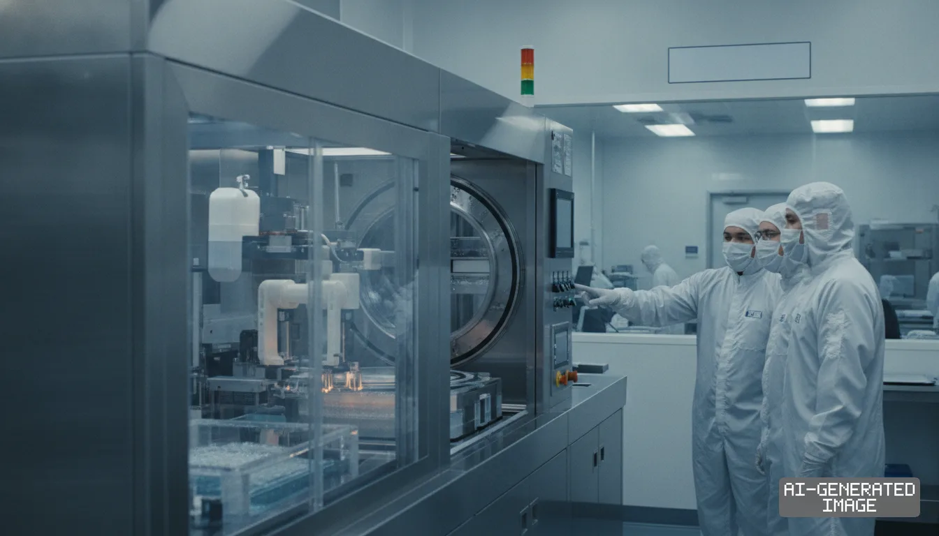
Samsung Electronics adopts three-track DRAM roadmap for sub-10nm chips
The architecture roadmap splits fabrication across hybrid bonding, planar scaling and vertical transistors to overcome sub-10nm scaling limits.

Samsung Electronics finalized a three-track architecture roadmap for next-generation sub-10-nanometer dynamic random-access memory on Nov. 17, dividing its fabrication strategy across wafer bonding, planar scaling and vertical transistors.
The structural pivot addresses physical limits below the 10-nanometer threshold. Patterning distortion, electrical leakage and capacitor aspect ratios have rendered uniform scaling across all memory categories increasingly impractical, company engineers confirmed in technical briefings.
Samsung held 41.5% of the global DRAM market by revenue in the second quarter, generating 14.2 trillion won ($10.3 billion) in segment sales. Preserving cost efficiency across diverse customer bases requires distinct manufacturing paths, the company said.
The first track, designated internally as D0A, introduces wafer-to-wafer hybrid bonding for sixth-generation high-bandwidth memory, known as HBM5. The architecture separates memory cells from periphery circuits, building them on separate 300-millimeter silicon wafers before bonding.
Under the D0A approach, Samsung fabricates memory cells on its proven D1b process. In contrast, the company routes the underlying core and periphery control logic to its denser D1d node, maximizing interface speeds.
Hybrid bonding attaches the two processed wafers directly with copper-to-copper interconnects. The scheme eliminates traditional microbumps, slashing interconnect pitches and bypassing the thermal penalties that accompany conventional through-silicon via stacking in high-density accelerator packages.
Samsung plans to apply the D0A scheme directly to HBM5 modules designed for artificial intelligence accelerators. The architecture expands silicon area dedicated purely to storage cells, delivering twice the operating bandwidth of seventh-generation HBM4E units.
The second track focuses on standard D1d planar scaling. Samsung will maintain its conventional 6F² cell layout — a standard hexagonal layout measuring six times the square of minimum feature size — on a single monolithic wafer.
The D1d design targets commodity DRAM and mobile low-power double data rate (LPDDR) chips. In these cost-sensitive markets, complex hybrid bonding packaging costs cannot yet be amortized across consumer device price tags, the company noted.
Shrinking the physical footprint of the 6F² layout on a unified substrate allows Samsung to preserve established assembly lines. The process relies on existing extreme ultraviolet (EUV) lithography scanners installed at its Pyeongtaek fabrication complex.
The third track, designated D0AV, represents an architectural break from planar memory. Samsung is engineering a 4F² cell layout paired with vertical channel transistors (VCT) to shrink cell surface areas by one third.
Vertical channel transistors rotate the current flow perpendicular to the silicon substrate, running vertically rather than horizontally. The vertical orientation prevents source-to-drain electrical punch-through, which degrades retention performance when cell spacing drops below 10 nanometers.
Samsung intends to deploy the D0AV structure across high-performance enterprise server modules by 2028. The architecture serves as the foundation before the company shifts toward fully stacked, multi-layer three-dimensional DRAM architectures late this decade.
The split strategy directly alters competitive dynamics against domestic rival SK hynix. SK hynix generated 53% of its operating profit from high-bandwidth memory in the third quarter, maintaining leading supply shares at Nvidia.
SK hynix is pursuing vertical gate structures to bridge its own sub-10-nanometer migration. Samsung’s decision to separate HBM5 fabrication from monolithic planar DRAM aims to neutralize packaging yields that slowed its initial HBM3E commercialization.
Wafer-to-wafer bonding requires specialized front-end and back-end equipment. Tokyo Electron supplies advanced dielectric deposition chambers, while Besi and Applied Materials lead hybrid copper bonding tools, linking tool procurements to Samsung's packaging capital budgets.
Samsung outlined parts of its vertical scaling concepts at the Future of Memory and Storage conference on Aug. 4. Executive Vice President Jin-Yub Lee showcased mock-ups of zHBM, a 3D memory stacked directly atop host processors.
At the SEMICON Taiwan executive summit on Sept. 1, Memory Product Planning Vice President Choi Jang-seok detailed the CUBE framework. The roadmap targets doubling HBM5 performance over HBM4E while reducing thermal resistance by 20%.
The three-track division permits Samsung to stage capital expenditure across multiple fiscal years. Rather than converting entire fabs to unproven vertical channel tools, the company limits high-risk tool orders to initial accelerator memory lines.
Samsung targets transferring both the D1d planar process and the D0A hybrid-bonded process to mass-production fabrication lines in the second half of 2027. Tool installation and pilot runs will take place at Pyeongtaek Line 4.
The company has not published formal regulatory filings confirming the D0A and D0AV node codenames, and cleanroom floor space allocation between foundry logic and memory bonding lines remains undisclosed.
Pilot wafer runs on the D0A hybrid bonding line will yield preliminary parametric test data in the first quarter of 2027, setting the baseline for customer sampling ahead of HBM5 server qualifications.
Impact map
How this development propagates across the region and out to global buyers.
| Event | Korea | China | Japan | Global impact |
|---|---|---|---|---|
| Sub-10nm DRAM three-track roadmap | Samsung balances D1d planar and D0A wafer bonding while SK hynix advances vertical gate 4F² | CXMT gains time in 6F² commodity DRAM as Korean leaders diversify packaging architectures | Tokyo Electron and packaging suppliers capture increased deposition and hybrid bonding tool spend | AI server BOM faces higher initial HBM5 wafer-bonding cost offset by 20% lower thermal resistance |
In this story
- Companies
- Samsung Electronics
- Tickers
- 005930.KS
- Exposed
- SK hynix
- Impact
- Supply ChainCapexCost Structure
Related briefings
- Dongjin Semichem operating profit jumps 51% on photoresist surge Also on SK hynix, Samsung Electronics, Cost Structure
- Korea Power Exchange splits wholesale rates to curb Seoul factory load Also on SK hynix, Samsung Electronics, Cost Structure
- TSMC and Samsung embed liquid microchannels into AI packages Also on SK hynix, Samsung Electronics, Cost Structure
- SK hynix speeds HBM4 design with Nvidia physics simulation tools Also on SK hynix, Samsung Electronics, Cost Structure
Sources
Reporting
Confidence: medium — how we grade this
The documents behind this briefing are linked above. East Asia Brief produces its English text with AI assistance under human editorial review, and does not translate or republish other outlets' articles. See our methodology and AI policy. Spotted an error? Tell us.
The Morning Brief
What changed in Korean, Chinese and Japanese industry overnight — and what it means for your supply chain. One email, weekday mornings, US time. Free.
The Morning Brief is in preparation. Leave your address and we will write to you once — when the first issue is ready. Nothing before that.