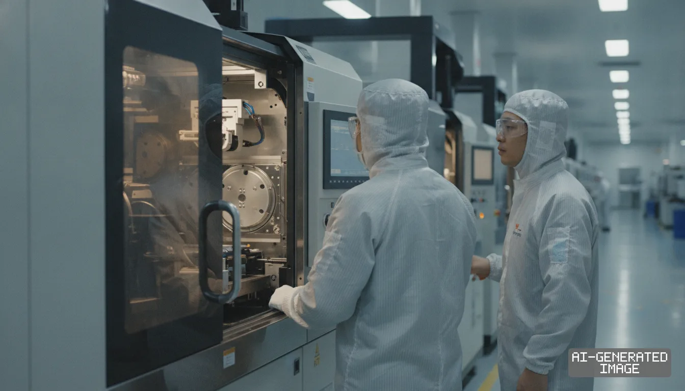
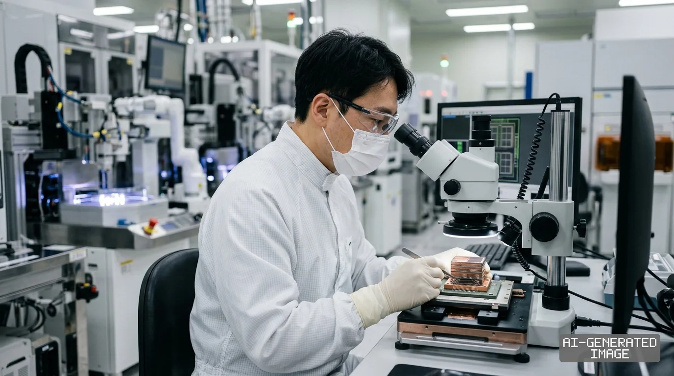
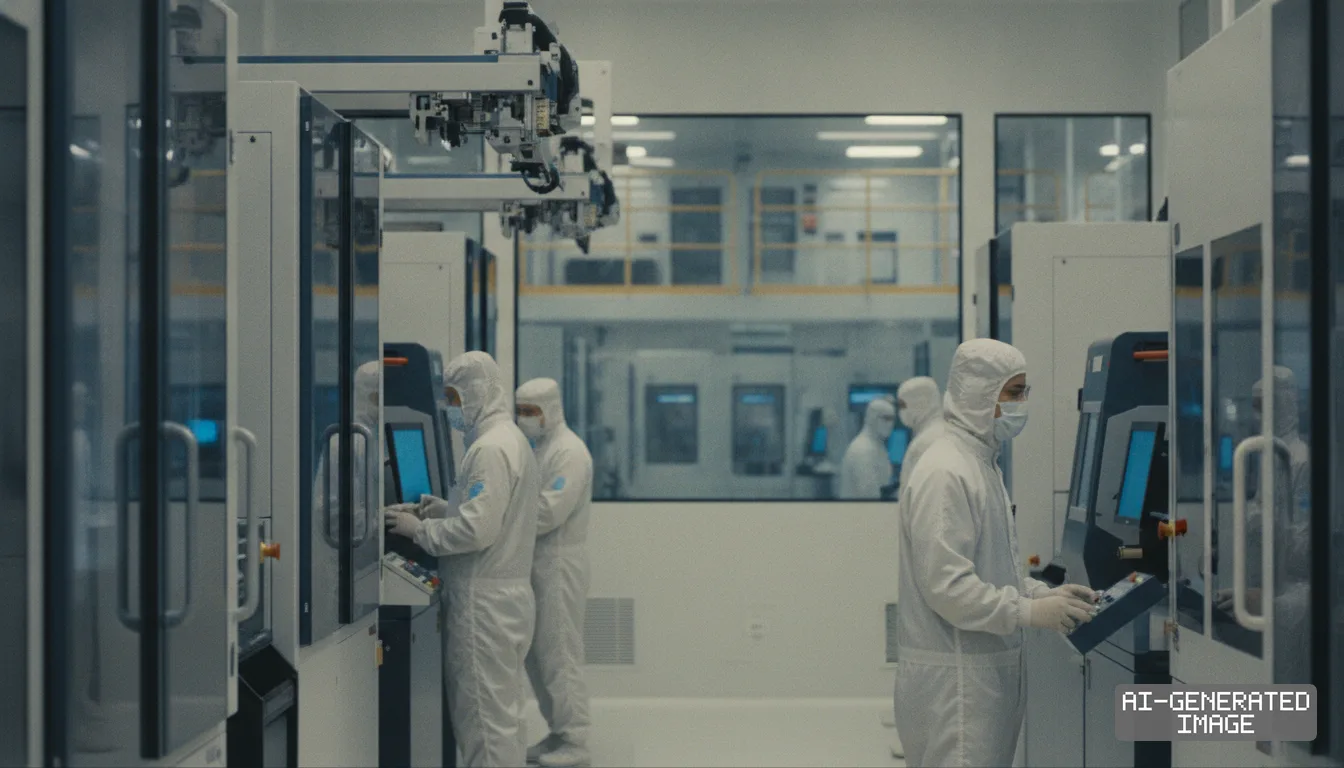
Skytech opens TSMC-backed advanced process lab to speed chip tool verification
The joint Taiwan facility focuses on thin-film deposition tools, film modification techniques and chemical precursor screening for next-generation wafer fabrication.
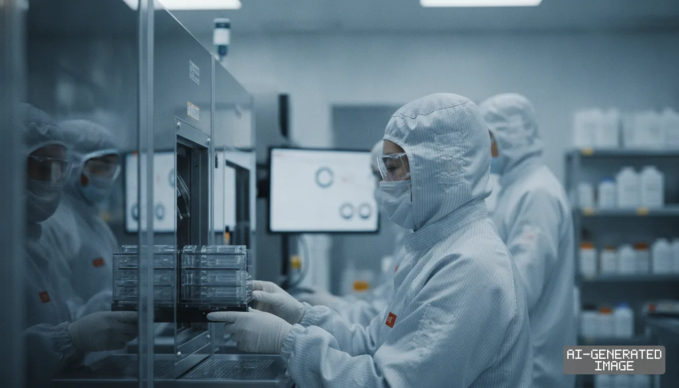
Skytech inaugurated an advanced semiconductor process laboratory in Taiwan on Sept. 1, 2026, partnering with Taiwan Semiconductor Manufacturing Co. to accelerate domestic equipment verification.
The facility establishes a dedicated co-development platform to evaluate thin-film deposition systems and specialty chemical precursors directly against the operating requirements of next-generation wafer fabrication lines.
TSMC, the world's largest dedicated contract chipmaker, has expanded its supplier development programs in Taiwan to shorten engineering feedback cycles and build out domestic equipment manufacturing capabilities.
The opening ceremony brought together senior leadership from both companies on Sept. 1. Dr. Chang Hsun-ming, TSMC vice president of research and development for advanced equipment and module development, represented the foundry.
Skytech attended with founder Luo Wei-rui, Chairman Huang Chien-lo and Chief Executive Officer Yi Chin-liang alongside the company's core engineering divisions.
The newly opened laboratory structures its technical program around three primary research tracks to address physical bottlenecks in sub-2-nanometer wafer processing.
The first track concentrates on advanced thin-film deposition equipment. Engineers will optimize locally designed physical vapor deposition and atomic layer deposition tools to meet tighter process tolerances required by next-generation chip architectures.
Thin-film deposition forms critical microscopic layers of conductive and insulating materials on silicon wafers. Process variations at this stage directly determine electrical performance and overall manufacturing yields at leading-edge nodes.
The second track focuses on thin-film property modification. Research teams will adjust deposition parameters to enhance film thickness uniformity, trench gap-filling precision and structural stability across complex three-dimensional transistor gates.
Yield margins at advanced nodes depend heavily on eliminating nanoscale voids during metal and dielectric filling. The lab will conduct iterative recipe tuning on production-grade substrates to resolve defects before volume tool installation.
The third track establishes a screening and qualification system for precursor chemicals. Precursors provide the active chemical elements required to grow functional thin films inside high-vacuum process chambers.
Skytech and TSMC will assess emerging specialty gases and organometallic compounds for thermal stability, reaction efficiency and chemical purity during early-stage synthesis.
The chemical evaluation process also incorporates environmental and workplace safety criteria. The partners aim to identify non-toxic, low-emission precursor formulations that comply with international sustainability standards prior to commercial adoption.
The opening of the laboratory represents a turning point for domestic semiconductor toolmakers, Skytech Chief Executive Officer Yi Chin-liang said Sept. 1.
Taiwanese suppliers are moving beyond reproducing standard fab machinery to become collaborative innovators working directly on frontier nodes, Yi said.
Skytech plans to expand its local research expenditure to deepen cooperation with regional component suppliers and support domestic tool production goals, Yi said.
Skytech manufactures semiconductor processing machinery, specializing in thin-film coating systems, wafer bonder modules and specialized packaging equipment.
Leading foundries have historically sourced more than 80% of their front-end thin-film and etch equipment from multinational vendors based in the United States, Japan and Europe.
Global equipment supply chains remain concentrated among major vendors, including Applied Materials, Lam Research, Tokyo Electron and ASML.
Collaborative development laboratories allow foundries to run rapid equipment modifications without interrupting high-volume manufacturing lines in commercial cleanrooms.
TSMC has increasingly supported domestic engineering partnerships to build secondary equipment sources closer to its primary fabrication hubs in Hsinchu, Taichung and Tainan.
Local tool qualification shortens tool customization lead times from months to weeks, enabling faster integration of novel process materials.
The initiative also assists domestic tool builders in acquiring operational data necessary to meet production standards set by global semiconductor manufacturers.
Skytech and TSMC have not disclosed the capital investment figure for the laboratory buildout or the specific cost-sharing terms behind the joint research operations.
The Advanced Process Laboratory commenced formal joint research and tool verification workflows immediately following the Sept. 1 inauguration.
Impact map
How this development propagates across the region and out to global buyers.
| Event | Korea | China | Japan | Global impact |
|---|---|---|---|---|
| Skytech process lab | — | — | — | front-end tool qualification |
In this story
- Companies
- SkytechTaiwan Semiconductor Manufacturing Co.
- Tickers
- 6937.TW2330.TW
- Exposed
- Applied MaterialsLam ResearchTokyo ElectronASML
- Policy
- Economic Security
- Impact
- Supply ChainCapexCompliance
Track every Economic Security development →
Related briefings
- Japan Linear Guide Makers Expand Ultra-Clean Units for 2nm Fab Robotics Also on Lam Research, Applied Materials, ASML
- ASML expands Japan workforce to 700 to support Rapidus 2nm and TSMC fabs Also on Lam Research, Applied Materials, ASML
- Taiwan clears TSMC fab site for sub-1.4nm chips at Longtan Also on Applied Materials, ASML, Tokyo Electron
- SK hynix seeks US export clearance for Wuxi memory equipment Also on Lam Research, Applied Materials, Compliance
Sources
Primary documents
Reporting
Confidence: high — how we grade this
The documents behind this briefing are linked above. East Asia Brief produces its English text with AI assistance under human editorial review, and does not translate or republish other outlets' articles. See our methodology and AI policy. Spotted an error? Tell us.
The Morning Brief
What changed in Korean, Chinese and Japanese industry overnight — and what it means for your supply chain. One email, weekday mornings, US time. Free.
The Morning Brief is in preparation. Leave your address and we will write to you once — when the first issue is ready. Nothing before that.