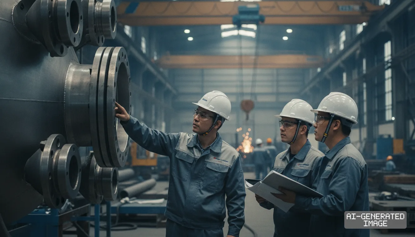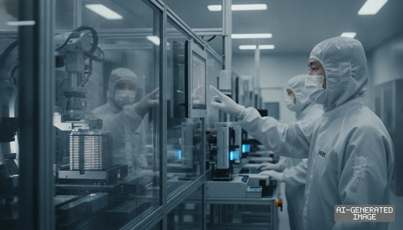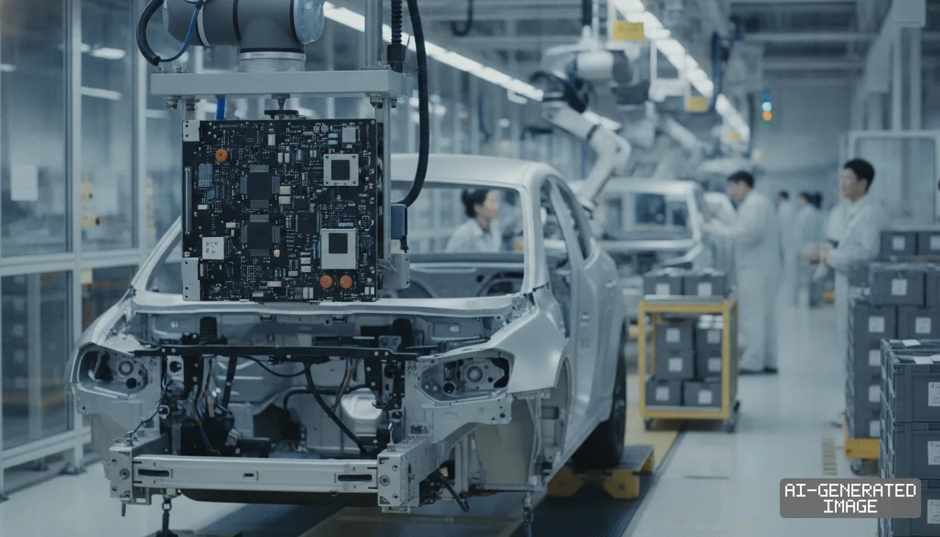
Samsung breaks ground on $33B advanced packaging fab in Asan
The Onyang Line 5 project commits 6 trillion won for construction and 40 trillion won for tool procurement across 31,000 square meters of cleanroom space.
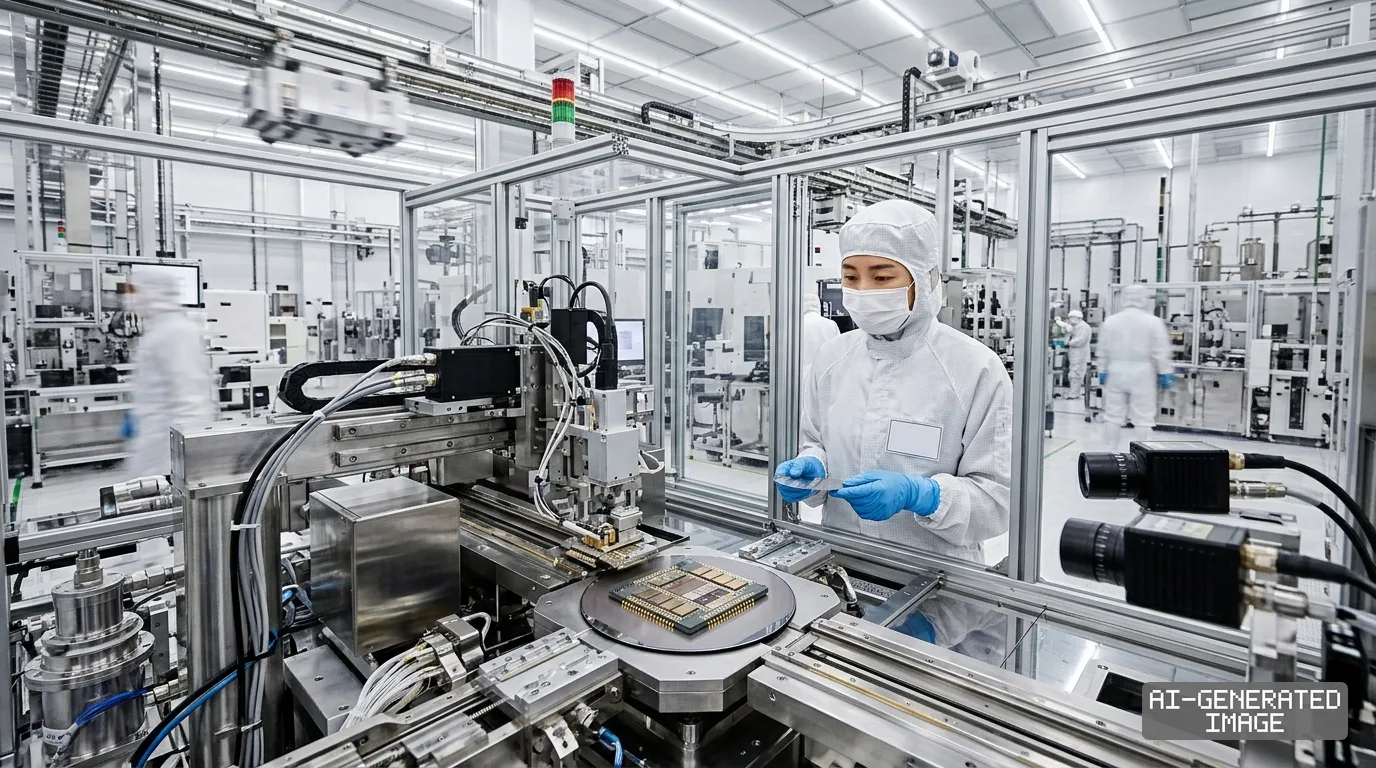
Samsung Electronics broke ground on a 46 trillion won ($32.9 billion) advanced packaging facility at its Onyang campus in Asan, South Korea, on Nov. 12, 2026.
The project commits 6 trillion won ($4.3 billion) to construct the Onyang Line 5 building. An additional 40 trillion won, equivalent to roughly $30 billion, will fund phased equipment procurement, government officials said.
The fab will feature 31,000 square meters of cleanroom floor space across three stories. The facility will expand the site's total floor area by 56% to 420,000 square meters, according to municipal planning records.
Construction requires an average of 3,400 workers daily. The project will generate 2.6 trillion won ($1.86 billion) in regional production effects and create 700 permanent manufacturing jobs, Asan municipal authorities said.
The plant will package next-generation high-bandwidth memory (HBM), stacking dynamic random-access memory dies vertically to accelerate data flow in artificial intelligence processors. Advanced packaging connects separate silicon dies on an intermediate silicon interposer.
Samsung aims to run backend lines for 16-high HBM4 and HBM4E units at the site. Those generations require sub-micron interconnects and hybrid bonding to prevent memory stacks from overheating during intensive model training.
The Onyang site had handled conventional memory assembly and final testing since late 1991. The facility will now operate as a primary high-bandwidth memory hub, Samsung Electronics Executive Chairman Lee Jae-yong said.
Samsung advanced its completion timetable by 12 months in response to tightening server memory backlogs. The company schedules initial line operations for June 2028 and targets commercial mass production for May 2029.
The buildout directly challenges Taiwan Semiconductor Manufacturing Co. (TSMC), which controls over 80% of global capacity in 2.5D advanced packaging. TSMC packages flagship graphics chips for Nvidia through its proprietary Chip-on-Wafer-on-Substrate technology.
Capacity constraints at TSMC have created a two-quarter bottleneck for global accelerator deliveries. Major chip designers have sought alternative packaging sources to alleviate reliance on Taiwanese backend factories, industry procurement filings indicate.
Domestic rival SK hynix supplies more than 50% of the world's high-bandwidth memory market. SK hynix relies on a foundry alliance with TSMC for its upcoming HBM4 units, outsourcing custom logic base wafer production.
Samsung plans to counter that alliance with an integrated turnkey service. The company fabricates core memory stacks, manufactures logic base dies on internal foundry lines and completes advanced 2.5D packaging within a unified corridor.
The Onyang project represents the largest single element of a 144 trillion won regional capital program outlined by Samsung Group. The four-affiliate program directs capital across semiconductor, display, substrate and battery manufacturing facilities.
Samsung Electronics will allocate 60 trillion won to memory and packaging lines across Asan and Cheonan. That figure includes capital expenditures for modernizing older backend facilities at the adjacent Cheonan campus.
Display affiliate Samsung Display will invest 67 trillion won in the region. That expenditure includes 5.9 trillion won ($4.2 billion) for its A7 organic light-emitting diode production line in Asan, scheduled for late 2029.
Component arm Samsung Electro-Mechanics is directing 4.3 trillion won toward a high-performance flip-chip ball grid array substrate plant in Sejong. The facility will produce high-density server packaging substrates starting September 2028.
Battery maker Samsung SDI will invest 9 trillion won to build an advanced engineering center in Cheonan. The site will test prototype cells and pilot production equipment for solid-state batteries.
The Ministry of Trade, Industry and Energy introduced the regional manufacturing blueprint on July 2, 2026. Thursday's ceremony marked the physical start of construction four months after the ministry published the development framework.
Asan municipal authorities established an inter-agency support team across 29 local divisions to accelerate building permits. The administrative intervention shortened review times by two thirds to enable pre-winter ground preparation.
Samsung Electronics has not published a standalone regulatory disclosure on the Korea Exchange detailing individual tool orders, and the company has not released vendor allocations across etching, bonding and deposition equipment.
Civil engineering and foundation pilings continue at the Asan site before structural cleanroom framing begins next year. The Ministry of Trade, Industry and Energy convenes its next public-private project review in Sejong in December.
Impact map
How this development propagates across the region and out to global buyers.
| Event | Korea | China | Japan | Global impact |
|---|---|---|---|---|
| Onyang Line 5 packaging fab | Samsung commits 46 trillion won, pulling commercial HBM operation forward to June 2028 | domestic AI designers face continued 2.5D packaging bottlenecks under external trade rules | tool makers Tokyo Electron and Disco see packaging equipment orders expand through 2028 | TSMC faces direct competition for AI accelerator packaging as Samsung offers turnkey memory and foundry lines |
In this story
- Companies
- Samsung Electronics
- Tickers
- 005930.KS
- Exposed
- TSMCSK hynixSamsung Electro-MechanicsSamsung DisplaySamsung SDI
- Policy
- Subsidies
- Impact
- CapexSupply ChainOrder Book
Track every Subsidies development →
Related briefings
- Samsung convenes 170 Hyundai executives for auto chip summit Also on Samsung Display, Samsung Electro-Mechanics, Samsung SDI
- Samsung SDI pushes Indiana battery plant after buying out GM stake Also on Samsung Display, Samsung SDI, Subsidies
- Samsung SDI buys GM stake in Indiana battery venture for ESS Also on Samsung Display, Samsung SDI, Subsidies
- Japan Display sells Mobara fab to Shinko for chip packaging Also on Samsung Display, Subsidies
Sources
Reporting
Confidence: medium — how we grade this
The documents behind this briefing are linked above. East Asia Brief produces its English text with AI assistance under human editorial review, and does not translate or republish other outlets' articles. See our methodology and AI policy. Spotted an error? Tell us.
The Morning Brief
What changed in Korean, Chinese and Japanese industry overnight — and what it means for your supply chain. One email, weekday mornings, US time. Free.
The Morning Brief is in preparation. Leave your address and we will write to you once — when the first issue is ready. Nothing before that.