China Substrate Makers Speed Glass Core Lines for AI Chips
BOE and domestic suppliers deployed automated through-glass via tools to challenge Korean rivals for next-generation semiconductor packaging contracts.
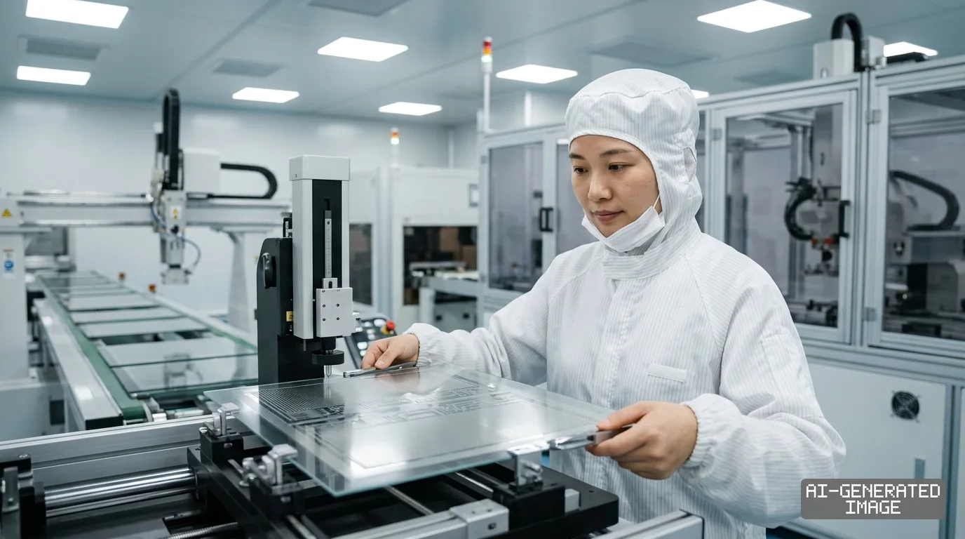
Chinese display and substrate manufacturers accelerated pilot line installations on Sept. 27, 2026, pulling forward qualification runs for glass-based semiconductor packaging to narrow the gap with South Korean front-runners.
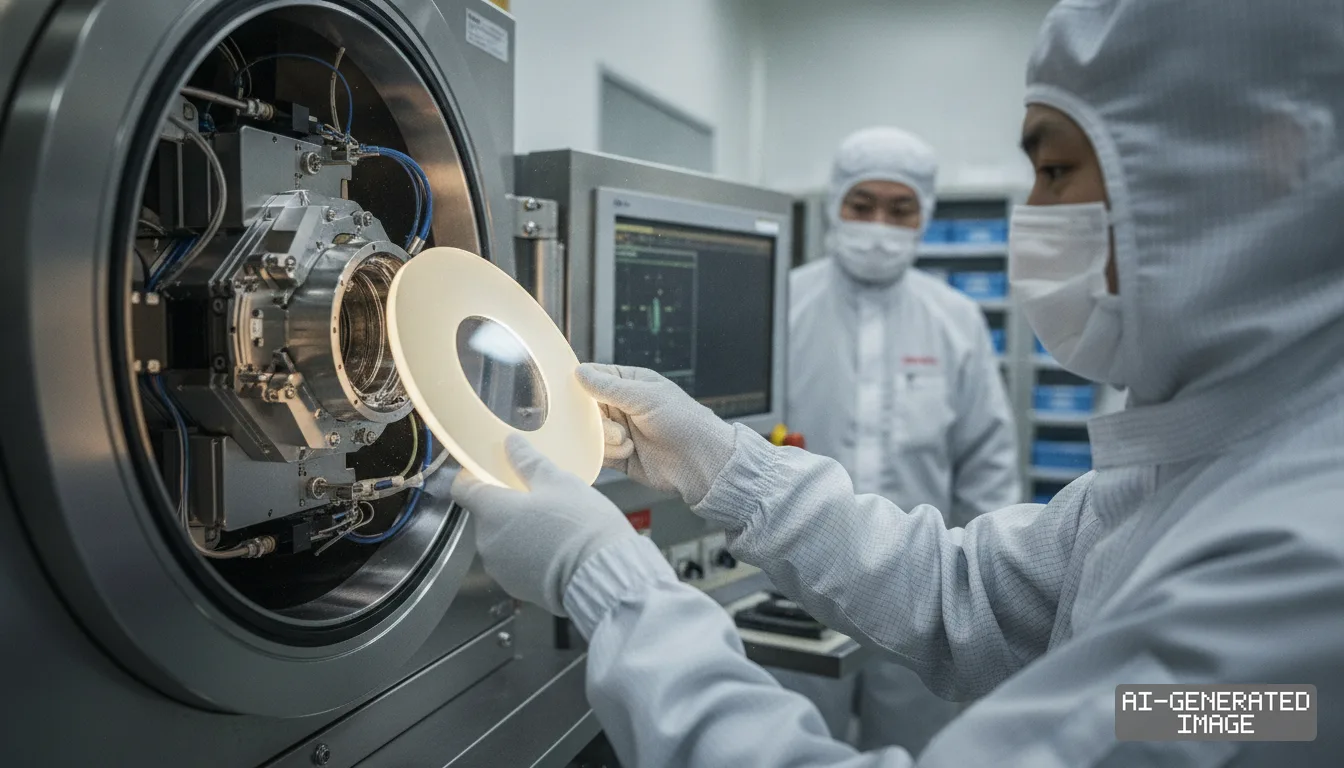
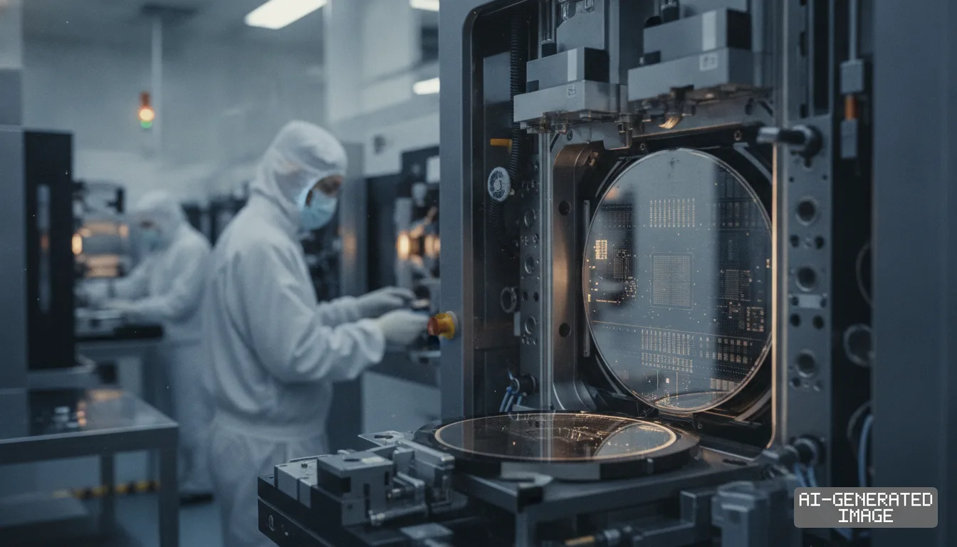
Glass core substrates replace traditional organic resin boards to carry artificial intelligence processors, eliminating heat-induced warping while supporting dense vertical electrical connections across multi-chiplet computing systems.
BOE Technology Group completed an automated pilot line sized for 1,000 panel substrates monthly, backing the installation with 993 million yuan ($140 million) in dedicated packaging capital.
The Beijing-based display leader displayed a through-glass via core board featuring an aspect ratio of 15:1. The component integrates 24 build-up wiring layers across a 1.0-millimeter plate with 67-micrometer holes.
Customer validation on sample units is underway with domestic processor designers. The company will finalize its commercial mass-production investment decision within one year, targeting the first half of 2027, Chairman Chen Yanshun said.
The pilot build follows an initial 390 million yuan expenditure in 2022 that created a wafer-level development platform. BOE combined display etching equipment with semiconductor plating tools to establish the full manufacturing sequence.
In 2025, BOE developed and sampled 20-layer glass carrier substrates configured in a 9-2-9 architecture. The format targets large artificial intelligence accelerators and high-performance computing chipsets.
Jiangxi WG Tech built a separate 100,000-square-meter annual capacity fabrication line through its Hubei Tonggewei unit. The company committed roughly 1.0 billion yuan ($141 million) to advance through-glass via processing for co-packaged optics.
The Jiangxi-based specialist achieved small-batch deliveries of glass carriers for chiplets and optical transceivers. However, depreciation and commissioning costs produced a net loss of 123 million yuan in the first half of 2026.
Technical disclosures show the unit drills vias with diameters as narrow as 3 micrometers and aspect ratios reaching 150:1. The facility processes 510-by-515-millimeter glass panels for high-density computing circuits.
Tianma Microelectronics confirmed its own development track in a Shenzhen Stock Exchange filing. The Shenzhen-based panel maker is fabricating glass packaging samples with supply chain partners, though work remains in the pre-research stage, according to the document.
The Chinese tool push challenges South Korea, where component makers established an initial commercialization lead. Absolics, an affiliate of SKC, built a 12,000-square-meter manufacturing plant in Covington, Georgia, to supply American computing customers.
The Georgia facility began pilot runs to deliver multi-chip packaging substrates. SKC aims to secure commercial production certification by late 2026, targeting initial revenues from top-tier artificial intelligence accelerator contracts.
Samsung Electro-Mechanics is constructing its own glass substrate trial line in Sejong, South Korea. The electronic component arm of Samsung Group plans to deliver customer prototypes in 2026 before entering mass production in 2027.
Glass substrates provide flat surfaces that resist distortion under thermal stress, unlike bismaleimide triazine and build-up film boards. They allow chipmakers to assemble larger processor modules containing more than eight chiplets.
Vertical through-glass via channels reduce high-frequency electrical signal loss by roughly 30% compared with conventional organic substrates. The material accommodates more than 10,000 vertical interconnects on a single processing package.
Chinese display manufacturers repurpose large-generation flat-panel fabrication lines to lower substrate production overhead. Their chemical etching and automated panel-handling systems transfer directly to panel-level semiconductor packaging operations.
Domestic equipment vendors supply laser drilling and copper deposition systems to Chinese pilot lines. Wuhan DR Laser and Han's Laser provide micro-via drilling machinery designed to bypass Western semiconductor export restrictions.
Specialty glass makers provide unpatterned raw sheets to local packagers. Shandong Linuo Technical Glass supplies borosilicate base panels, while Dinglong supplies chemical mechanical polishing pads for surface planarization steps.
Beyond domestic firms, international chipmakers are exploring Chinese manufacturing infrastructure. Intel formed a strategic partnership with Lens Technology in July 2026 to evaluate glass core substrate manufacturing.
Taiwanese packaging ecosystems are responding by integrating panel-level packaging assets. Display makers Innolux and AUO are converting older liquid-crystal display lines into fan-out panel-level packaging facilities.
Industry research group Omdia projects the global glass substrate market will reach $18.6 billion by 2026. Projections indicate global packaging demand will expand beyond $32.0 billion by 2030 as data centers adopt optical switches.
For artificial intelligence server manufacturers, Chinese entry introduces a parallel procurement base. Cloud operators could access lower-cost glass interposers for domestic computing clusters, reducing reliance on North American packaging lines.
Yield stability remains a hurdle for volume adoption. Glass is brittle and prone to micro-cracking during vacuum lamination, high-temperature copper annealing and panel singulation cuts, according to packaging engineers.
The corporate filings do not state the baseline production yield across the automated lines, and manufacturers have not named their pilot computing customers.
Chinese packaging houses will submit sample test results to domestic chip designers before December. Commercial supply agreements hinge on qualification trials scheduled across the first six months of 2027.
Impact map
How this development propagates across the region and out to global buyers.
| Event | Korea | China | Japan | Global impact |
|---|---|---|---|---|
| Glass substrate pilot line expansion | Absolics and Samsung Electro-Mechanics face compressed commercialization windows for 2026-2027 deliveries | BOE and WG Tech leverage domestic display tool lines to build 100,000-square-meter TGV capacity | Raw substrate makers including AGC and NEG see shifting customer mix toward Chinese pilot fabs | AI server designers gain alternate, lower-cost packaging sources for multi-chiplet computing architectures |
In this story
- Companies
- BOE Technology GroupJiangxi WG TechTianma MicroelectronicsSKCSamsung Electro-Mechanics
- Tickers
- 000725.SZ603773.SH000050.SZ011790.KS009150.KS
- Exposed
- IntelLens TechnologyWuhan DR Laser
- Policy
- SubsidiesExport Controls
- Impact
- Supply ChainCapexCost Structure
Track every Subsidies development → Track every Export Controls development →
Related briefings
- South Korean substrate makers develop embedded silicon bridges for AI chips Also on Samsung Electro-Mechanics, Intel, Cost Structure
- Ibiden and Shinko ramp high-layer FC-BGA lines as AI server package sizes expand Also on Samsung Electro-Mechanics, Intel, Cost Structure
- South Korean toolmakers advance glass substrate TGV laser drillers to volume lines Also on Samsung Electro-Mechanics
- SK hynix subsidiary Solidigm weighs NAND fab in New York Also on Intel, Export Controls
Sources
Reporting
Confidence: medium — how we grade this
The documents behind this briefing are linked above. East Asia Brief produces its English text with AI assistance under human editorial review, and does not translate or republish other outlets' articles. See our methodology and AI policy. Spotted an error? Tell us.
The Morning Brief
What changed in Korean, Chinese and Japanese industry overnight — and what it means for your supply chain. One email, weekday mornings, US time. Free.
The Morning Brief is in preparation. Leave your address and we will write to you once — when the first issue is ready. Nothing before that.