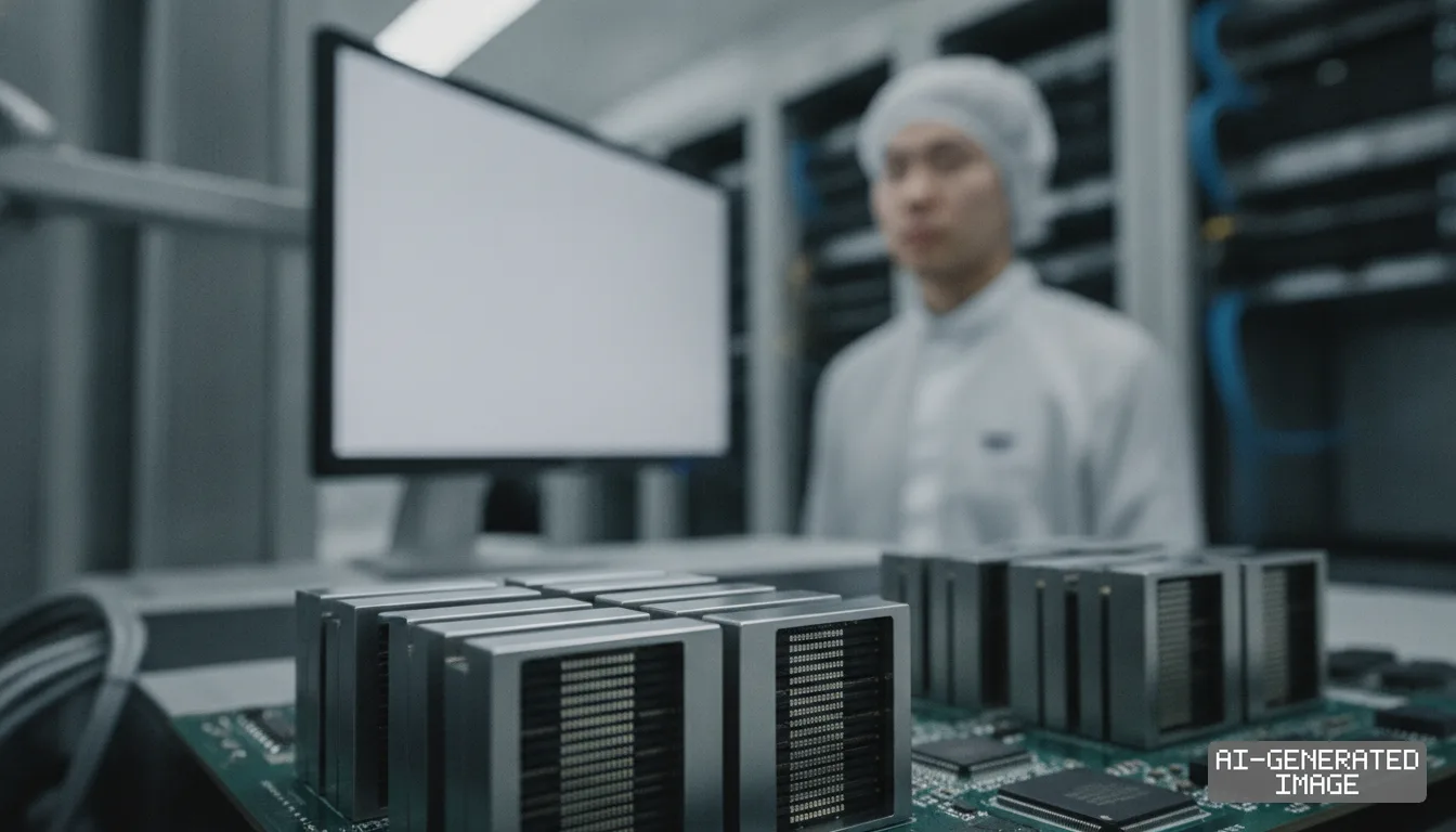
AMD Reaffirms TSMC Alliance While Evaluating Rival Foundries
The chip designer projected an AI market of up to $3 trillion by 2030, keeping its wafer volume anchored at TSMC while conducting due diligence on competing packaging providers.
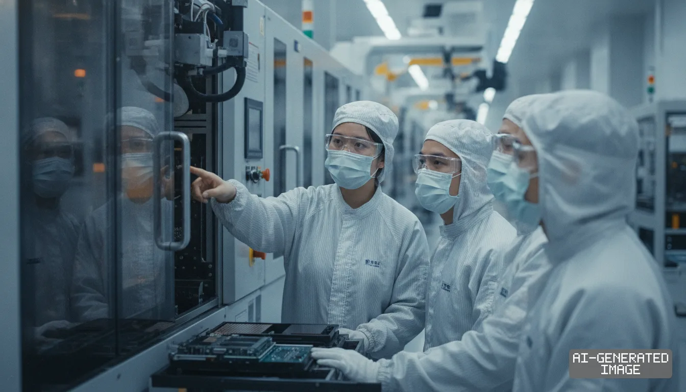
Advanced Micro Devices reaffirmed on Sept. 12 that Taiwan Semiconductor Manufacturing Co. will remain its primary foundry partner, dampening speculation of an imminent manufacturing shift to Intel Foundry.
Chief Financial Officer Jean Hu lifted AMD's market forecast for artificial intelligence chips to $3 trillion by 2030. The company expects its data center revenue to reach roughly $70 billion next year, Hu said.
TSMC fabricates all of AMD's commercial graphics processing units and server central processing units. The Taiwanese contract manufacturer controls more than 85% of worldwide capacity for advanced packaging lines needed in artificial intelligence accelerators.
Tight capacity persists across silicon wafers, advanced packaging and high-bandwidth memory. AMD relies on TSMC production lines to support volume shipments of its Instinct accelerator family to cloud computing operators, Hu said.
Matt Ramsay, corporate vice president of financial strategy and investor relations at AMD, outlined the company's procurement policy. The designer evaluates every vendor in the market for advanced wafers and advanced packaging, Ramsay said.
The working relationship with TSMC will continue for the foreseeable future, Ramsay said. Long development cycles and technical integration anchor AMD's high-performance processor roadmap to TSMC manufacturing nodes through the end of the decade.
AMD co-develops process technology directly with TSMC rather than selecting standard foundry offerings off the shelf. That joint engineering spans three-dimensional packaging architectures, transistor scaling and power distribution networks, Hu said.
Market interest in alternative foundries surged after Northland Capital Markets upgraded Intel with a $120 price target. The brokerage pointed to potential foundry gains, sending Intel stock up 9% to $104.47 during Tuesday trading.
Speculation centered on advanced packaging rather than front-end wafer fabrication. UBS told clients that capacity bottlenecks at TSMC packaging facilities could push fabless customers toward Intel's embedded multi-die interconnect bridge technology by 2027.
Packaging represents the primary production constraint for artificial intelligence hardware. AMD uses chip-on-wafer-on-substrate packaging from TSMC, where delivery queues remain constrained despite factory construction across central and southern Taiwan.
Second-sourcing packaging allows fabless designers to mitigate production pauses without abandoning their primary wafer foundries. Dividing front-end lithography from back-end assembly provides operational flexibility against single-source vulnerabilities.
AMD is also diversifying component sourcing across memory partners. The designer selected Samsung Electronics to supply sixth-generation high-bandwidth memory for its upcoming MI450 series accelerators, securing high-density stacks for data center deployments.
The company's next-generation Helios infrastructure rack requires 432 gigabytes of high-bandwidth memory per node. Strong customer reservations for Helios in 2027 have exceeded initial internal forecasts, Hu said.
High memory requirements amplify cost pressures across the bill of materials. Keeping competitive pressure on manufacturing suppliers prevents foundry vendors from capturing outsized margins as artificial intelligence hardware budgets expand.
Publicly assessing alternative foundries functions as a bargaining tool against TSMC. The Taiwanese contract chipmaker implemented price increases on sub-5-nanometer wafers, citing elevated electricity tariffs and cleanroom construction costs in overseas facilities.
Chief Executive Officer Lisa Su maintained a similar procurement stance late last year. The designer keeps dialogue open with alternative foundries while preserving its manufacturing alliance with TSMC, Su said in earlier remarks.
Switching foundry partners remains difficult for high-performance computing logic. Porting existing designs from TSMC process libraries to Intel 18A or 14A nodes requires re-engineering physical layouts, redesigning custom cells and repeating qualification cycles.
AMD is expanding geographic diversity through TSMC's international fabrication sites. The company plans to tap TSMC's manufacturing facilities in Arizona, securing domestic United States wafer production without altering its foundry process recipes.
Intel Foundry continues to seek flagship commercial customers to validate its multi-billion-dollar factory network. Securing packaging orders from AMD would validate its external foundry operations, though commercial agreements remain elusive.
AMD has not executed any commercial wafer supply agreement or process test contract with Intel Foundry. Regulatory filings disclose no binding purchase commitments with external manufacturing facilities outside TSMC, leaving packaging speculation unconfirmed.
Production ramp for the MI450 accelerator series begins in October 2026. The deployment will test TSMC's packaging allocation ahead of high-volume deliveries scheduled throughout fiscal 2027.
Impact map
How this development propagates across the region and out to global buyers.
| Event | Korea | China | Japan | Global impact |
|---|---|---|---|---|
| AMD foundry dual-sourcing evaluation | Samsung Electronics supplies HBM4 memory for MI450 while competing for secondary packaging | Chinese hyperscalers face constrained AI accelerator allocations as TSMC packaging stays tight | Advantest and Ibiden maintain packaging test tool and substrate backlogs for TSMC supply chain | Chip designers preserve dual-sourcing rhetoric to cap TSMC wafer and packaging price increases |
In this story
- Companies
- Advanced Micro DevicesTaiwan Semiconductor Manufacturing Co.Intel Corporation
- Tickers
- AMDTSMINTC
- Exposed
- Samsung ElectronicsNvidia
- Policy
- Economic SecuritySubsidies
- Impact
- Supply ChainPricingCapex
Track every Economic Security development → Track every Subsidies development →
Related briefings
- Lasertec ships EUV pellicle defect inspection tools for sub-2nm chip production Also on Intel Corporation, Samsung Electronics
- Silicon interposer scaling drives foundry and OSAT shifts in 3.5D chiplets Also on Advanced Micro Devices, Taiwan Semiconductor Manufacturing Co, Samsung Electronics
- Ibiden and Shinko ramp high-layer FC-BGA lines as AI server package sizes expand Also on Advanced Micro Devices, Nvidia
- TSMC Reaffirms 2028 Target for 1.4nm Chips at Taichung Fab Also on Taiwan Semiconductor Manufacturing Co, Nvidia, Samsung Electronics
Sources
Primary documents
Reporting
Confidence: high — how we grade this
The documents behind this briefing are linked above. East Asia Brief produces its English text with AI assistance under human editorial review, and does not translate or republish other outlets' articles. See our methodology and AI policy. Spotted an error? Tell us.
The Morning Brief
What changed in Korean, Chinese and Japanese industry overnight — and what it means for your supply chain. One email, weekday mornings, US time. Free.
The first issue goes out shortly. Sign up now and you will not miss it.