Sumitomo Bakelite expands Asian chip molding compound lines
New production lines in Suzhou and Singapore will double mold underfill capacity and triple granular compound output to supply advanced artificial intelligence processors.
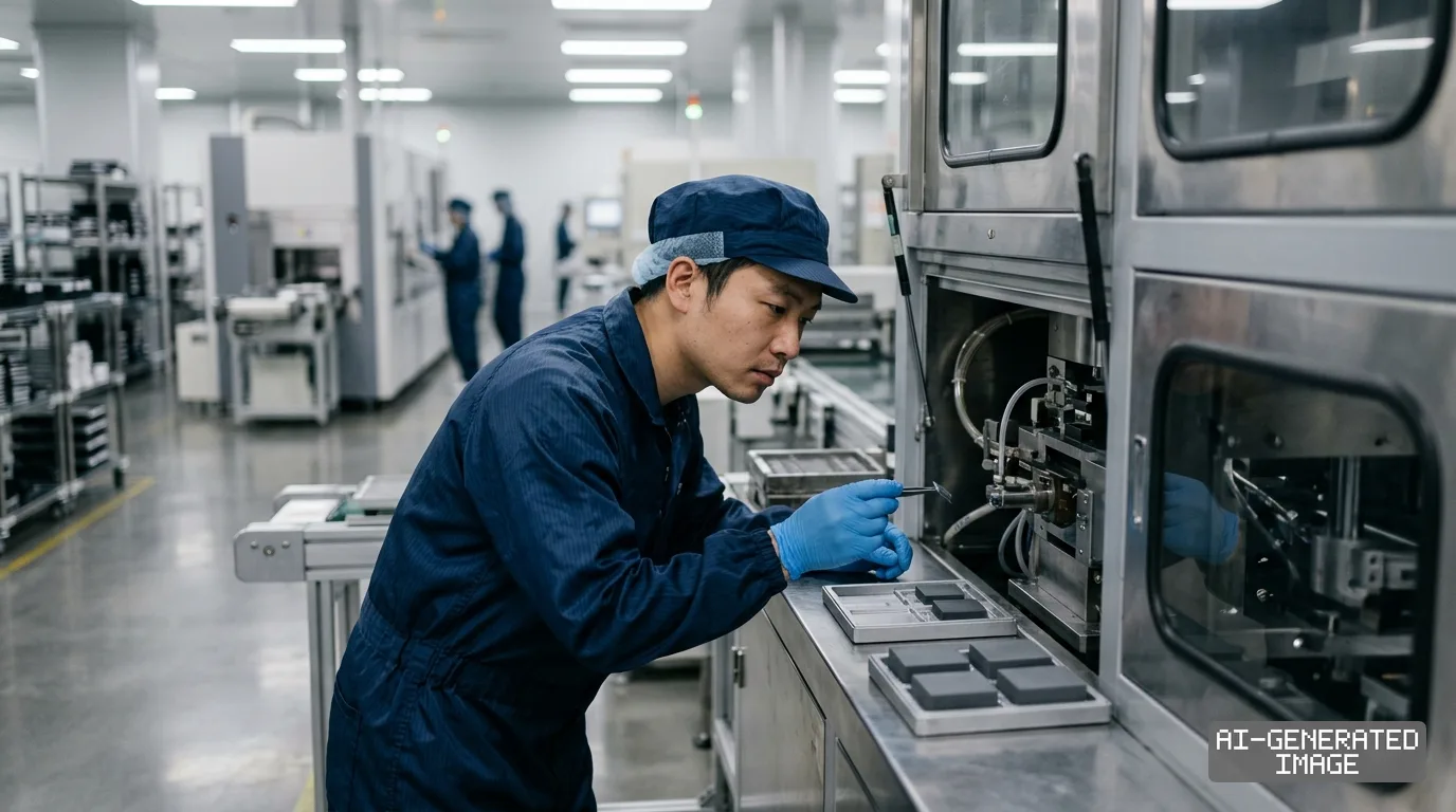
Sumitomo Bakelite announced Oct. 8, 2026, that it will install new packaging material production lines in China and Singapore to double its output of advanced semiconductor encapsulants.
The Tokyo-based materials manufacturer controls roughly 40% of the global market for epoxy molding compounds. The products provide physical protection, electrical insulation and heat dissipation for microchips mounted inside electronic systems.
The capital program will approximately double the company's production capacity for mold underfill materials. It will also approximately triple its manufacturing capacity for compression-molding granules compared with current operating levels.
Mold underfill — resin injected between stacked silicon dies and package substrates — prevents thermal fatigue. The compound fills microscopic clearances around copper microbumps while encapsulating the entire package.
Compression-molding granules serve large-format panel-level packaging and wafer-level packaging lines. The solid compound melts under heat to encase oversized artificial intelligence accelerator modules in a single curing cycle.
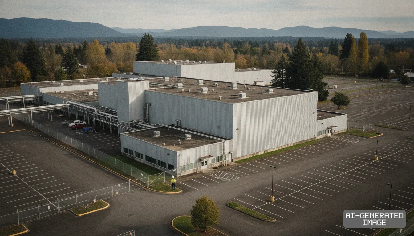
In Singapore, the company will install the new production lines within its existing manufacturing plant on Senoko South Road. Commercial production at the Southeast Asian facility is scheduled to begin at the end of fiscal 2028.
The unit, Sumitomo Bakelite Singapore Pte. Ltd., has produced semiconductor encapsulation resins since 1989. The facility supplies packaging lines across Southeast Asia, where multinational chipmakers cluster testing and assembly plants.
In China, the manufacturer will construct a new building within the factory site completed in 2024. Sumitomo Bakelite (Suzhou) Co., Ltd. plans to begin mass production on the new lines in fiscal 2030.
The Suzhou expansion is distinct from an earlier capacity project announced on June 25, 2026. That earlier program aimed to lift capacity for conventional molding compounds by about 30% by December 2028.
The October plan concentrates entirely on specialized high-performance grades for artificial intelligence processors and automotive electronics. The company markets these advanced formulations under its SUMIKON EME and SUMIKON EME Version GR product families.
The capacity additions will combine with the planned acquisition of Kyocera Corporation's chemical business. Sumitomo Bakelite agreed on Jan. 22 to acquire the unit and expects the share transfer to take effect on Oct. 30.
The transaction will absorb Kyocera's manufacturing operations for epoxy molding compounds, die-attach bonding pastes and industrial resins. It will also integrate Kyocera's existing production capacity for mold underfills and granular compounds.
The combined network gives Sumitomo Bakelite manufacturing plants for advanced encapsulants across Japan, China, Singapore, Taiwan and Belgium. This distributed structure allows the group to supply regional assembly hubs without crossing trade barriers.
Outsourced semiconductor assembly and test contractors represent the primary customer base for the expanded lines. ASE Technology Holding, the world's largest packaging contractor, operates high-volume facilities in Taiwan, China and Singapore.
ASE Technology Holding and peer packaging contractors consume Japanese molding resins across high-density computing lines. Packaging contractors require qualification testing of six to 12 months before adopting newly formulated epoxy compounds on volume lines.
Advanced packaging demand is expanding rapidly as generative artificial intelligence accelerators incorporate multiple high-bandwidth memory stacks. Dense clusters of silicon generate intense operational heat that causes substrate warping during thermal cycles.
To prevent warpage across large package footprints, assembly engineers are shifting away from liquid underfills. Mold underfills and granular compression resins allow uniform encapsulation across wider surface areas without leaving voids.
Automotive semiconductors are adding secondary pressure to high-temperature resin capacity. Electric vehicle powertrains and driver-assistance computers require high-glass-transition-temperature resins that withstand continuous operating temperatures above 175 degrees Celsius.
Local Chinese chemical manufacturers are developing domestic epoxy compounds to supply local foundries. Sumitomo Bakelite executives said in August that regional competition is intensifying, requiring faster deployment of advanced formulations.
The official company notice does not state the capital expenditure figure for the project. Financial news services reported the combined investment at roughly $63 million.
Sumitomo Bakelite will complete the Kyocera acquisition on Oct. 30, 2026. Commercial output from the Singapore line is scheduled for early 2029, followed by the Suzhou facility in fiscal 2030.
Impact map
How this development propagates across the region and out to global buyers.
| Event | Korea | China | Japan | Global impact |
|---|---|---|---|---|
| Sumitomo Bakelite packaging materials expansion | memory makers secure secondary sourcing for HBM mold underfills | Suzhou line adds domestic MUF supply by fiscal 2030, cutting import reliance | Sumitomo Bakelite secures roughly 40% global share across advanced packaging nodes | OSAT packaging houses gain dual-hub resin supply outside single-country chokepoints |
In this story
- Companies
- Sumitomo Bakelite
- Tickers
- 4203.T
- Exposed
- KyoceraASE Technology Holding
- Policy
- Economic Security
- Impact
- Supply ChainCapexCost Structure
Track every Economic Security development →
Related briefings
- Japanese epoxy mold makers reformulate resins to tame warpage in 16-high memory Also on Sumitomo Bakelite, Cost Structure
- METI Pools Factory Machine Data to Train Physical AI Models Also on Kyocera, Cost Structure
- Kyocera opens 68 billion yen Nagasaki plant for AI chip packaging Also on Kyocera
- Silicon interposer scaling drives foundry and OSAT shifts in 3.5D chiplets Also on ASE Technology Holding, Cost Structure
Sources
Reporting
Confidence: medium — how we grade this
The documents behind this briefing are linked above. East Asia Brief produces its English text with AI assistance under human editorial review, and does not translate or republish other outlets' articles. See our methodology and AI policy. Spotted an error? Tell us.
The Morning Brief
What changed in Korean, Chinese and Japanese industry overnight — and what it means for your supply chain. One email, weekday mornings, US time. Free.
The Morning Brief is in preparation. Leave your address and we will write to you once — when the first issue is ready. Nothing before that.