SK hynix taps HanmiGlobal for $4B Indiana HBM packaging fab
The project management contract solidifies construction of America's first advanced AI memory facility in West Lafayette ahead of cleanroom completion in October 2028.
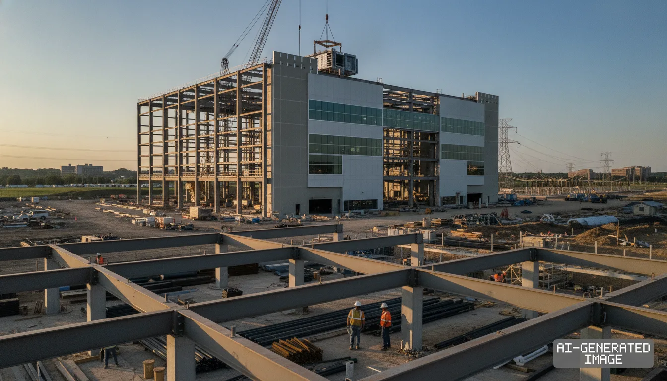
HanmiGlobal said Sept. 21, 2026 it is managing construction of SK hynix's $4 billion advanced packaging plant in West Lafayette, Indiana, to produce high-bandwidth memory for American artificial intelligence customers.
The facility represents a total capital commitment of more than $4 billion (5.5 trillion won). It spans 133.5 acres at the Purdue Research Park and marks the first advanced packaging hub for memory chips on American soil.
The project is expected to create roughly 7,000 direct and indirect jobs across construction, engineering and plant operations. About 1,000 permanent technical positions will run the completed cleanrooms and research facilities, according to company estimates.
HanmiGlobal began work on the project during the pre-construction phase in August 2024. The Seoul-based engineering manager oversaw early planning, cost modeling and initial design reviews before physical groundwork started in Tippecanoe County.
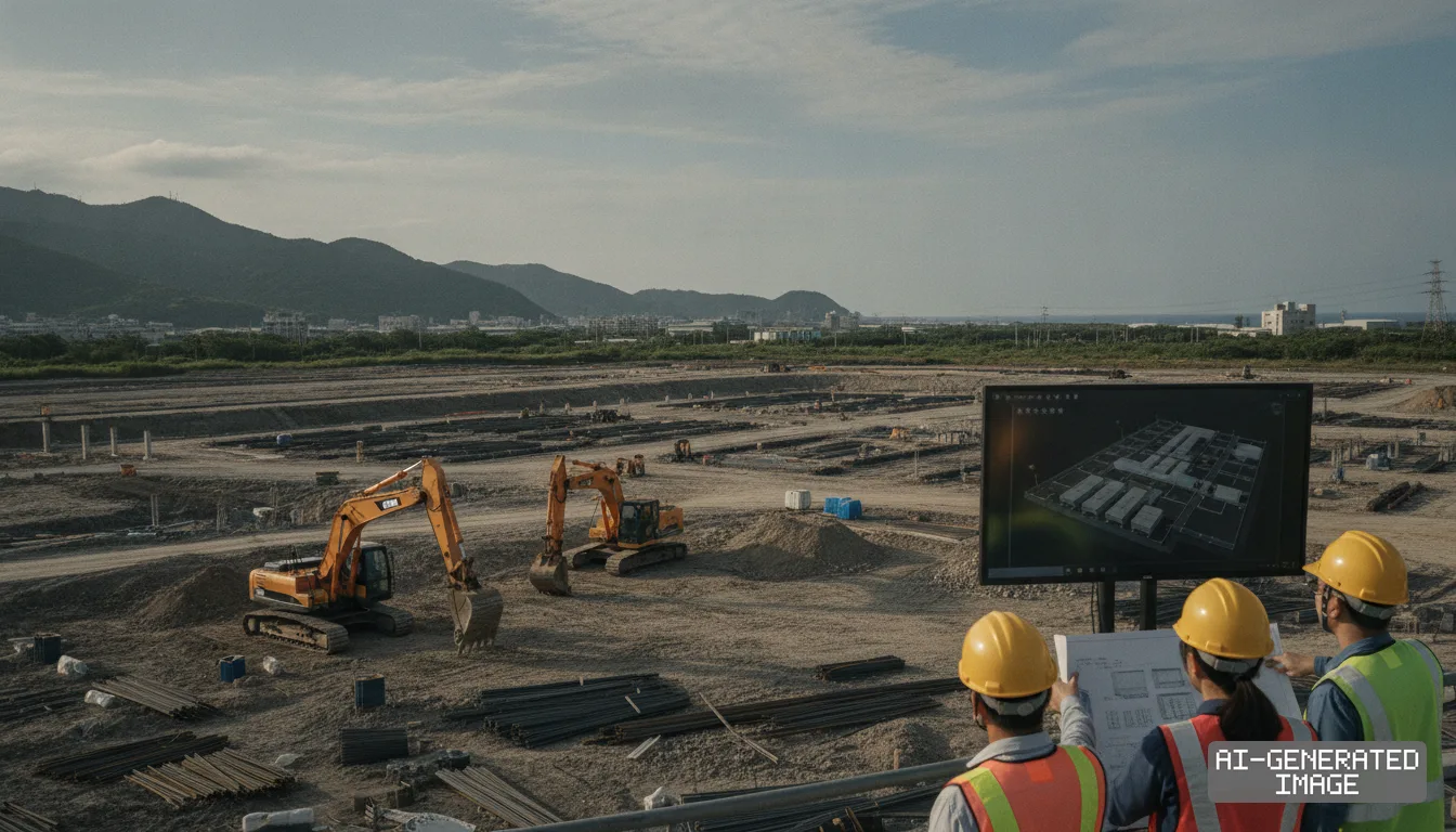
Heavy earthmoving crews began site excavation in March 2026. SK hynix then held an official groundbreaking ceremony on Aug. 27 at Purdue University's Holloway Gymnasium to signal the start of structural facility work.
Under the management mandate, HanmiGlobal directs all construction supervision through cleanroom completion in October 2028. Its duties cover architectural scheduling, cost controls, cleanroom compliance, site safety and contractor risk management.
The management specialist also coordinates technical integration between South Korean engineering suppliers and American general contractors. More than 100 supply chain vendors are tied to the plant build, the firm said.
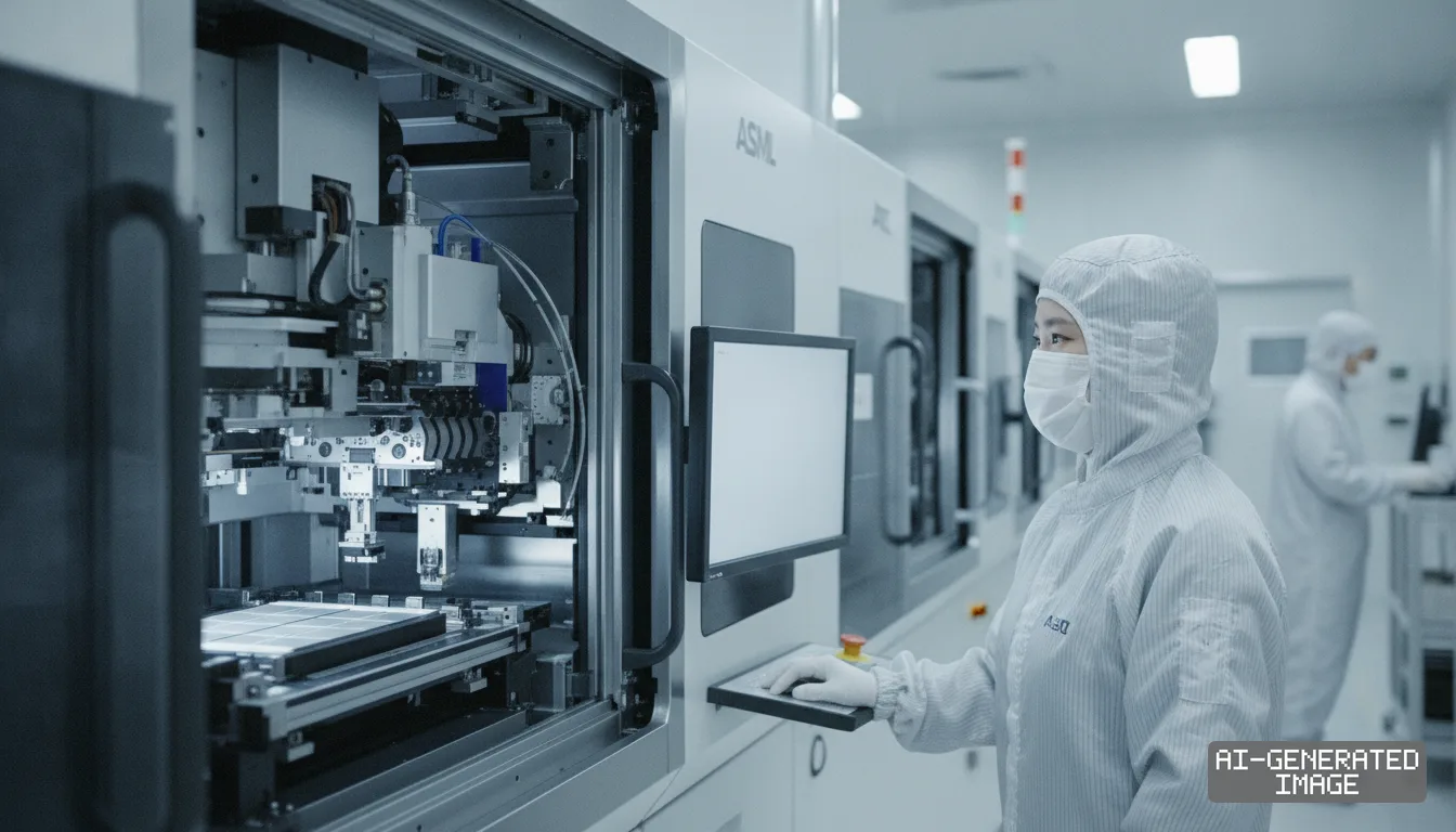
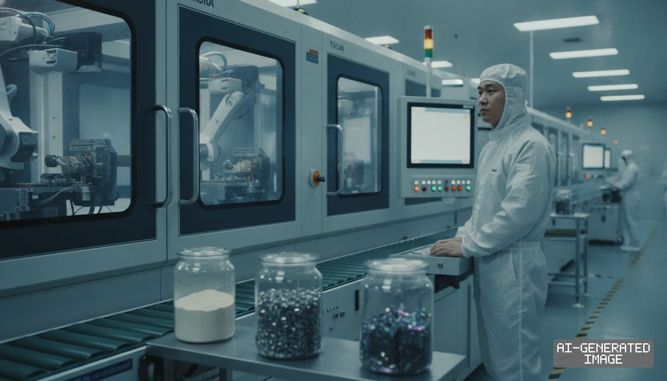
High-bandwidth memory, known as HBM, stacks dynamic random-access memory dies vertically using microscopic through-silicon vias. The architecture allows graphic processing units to ingest massive data volumes at multi-terabyte speeds needed for artificial intelligence workloads.
Advanced packaging has become the primary bottleneck in artificial intelligence hardware. Stacking dies closely together allows chip designers to bypass physical scaling limits of conventional silicon lithography without shrinking transistor gates further.
SK hynix plans to fabricate processed DRAM wafers at its high-volume cleanrooms in Icheon and Cheongju, South Korea. Workers will ship the tested wafers to West Lafayette for wafer-level packaging, stacking and final testing.
The finished memory modules will go directly to North American system makers, including Nvidia. Cutting transit times across the Pacific reduces delivery cycle times by several weeks for server assemblers.
The plant links directly to federal reshoring subsidies under the CHIPS and Science Act. The U.S. Department of Commerce awarded SK hynix up to $458 million in direct grant funding, alongside access to $500 million in government loan authority.
SK hynix also plans to seek a federal investment tax credit worth up to 25% of qualified capital expenditures from the U.S. Department of the Treasury. That credit could yield close to $1 billion in capital expenditure relief for the company.
The Department of Commerce tied disbursement of the $458 million grant to concrete construction milestones. Federal administrators inspect build progress before releasing each scheduled funding tranche, according to award terms.
The project deepens technical cooperation with Purdue University and regional educational institutions. SK hynix and Purdue signed an agreement to conduct joint packaging research and establish specialized workforce training programs on campus.
The university collaboration focuses on heterogeneous integration, thermal dissipation materials and memory-centric architectures. Researchers will use an on-site packaging research testbed to develop next-generation memory prototypes.
Building advanced cleanrooms in the United States presents acute cost and execution hurdles for Asian semiconductor companies. Local zoning codes, specialized utility hookups and union work rules have repeatedly stretched project budgets across North America.
HanmiGlobal has built an extensive portfolio managing U.S. capital projects for South Korean manufacturers. The company manages more than 20 advanced industrial facility projects across the country, including electric vehicle battery and undersea power cable plants.
Experience with American permitting procedures and local contracting practices helps insulate foreign clients from schedule slippage, the management firm said. Similar cross-border industrial builds in the southern states have faced multi-year delays over utility and labor friction.
The project management notice does not state the exact fee HanmiGlobal receives for managing the Indiana build. Regulatory filings submitted to South Korea's Financial Supervisory Service do not disclose the value of the service contract.
What happens next is the structural erection of the primary manufacturing building. HanmiGlobal is scheduled to deliver the fully qualified cleanroom shell to SK hynix in October 2028 for tool installation.
SK hynix plans to begin commercial mass production of next-generation HBM at the West Lafayette facility in the second half of 2029. Commercial shipments will follow qualification testing by major American customers.
Impact map
How this development propagates across the region and out to global buyers.
| Event | Korea | China | Japan | Global impact |
|---|---|---|---|---|
| SK hynix Indiana packaging plant construction | SK hynix establishes its first US back-end facility, shifting advanced wafer packaging closer to North American buyers | Mainland packaging vendors face exclusion from Tier-1 US AI server supply channels | Tool suppliers including Tokyo Electron and DISCO gain back-end equipment installation targets in Indiana | AI server supply chain cuts transpacific logistics lag for finished HBM modules by several weeks |
In this story
- Companies
- SK hynixHanmiGlobal
- Tickers
- 000660.KS053690.KQ
- Exposed
- NvidiaPurdue Research Foundation
- Policy
- SubsidiesTax CreditsEconomic Security
- Impact
- Supply ChainCapexCompliance
Track every Subsidies development → Track every Tax Credits development → Track every Economic Security development →
Related briefings
- SK hynix starts $4 billion packaging plant in Indiana to feed US AI Also on Tax Credits, Nvidia, SK hynix
- South Korea funds advanced chip packaging and backside power pilot lines Also on Tax Credits, SK hynix
- South Korean substrate makers develop embedded silicon bridges for AI chips Also on Tax Credits, SK hynix
- Comparing East Asia Fab Subsidies Across Japan, Korea, and China Also on Tax Credits, SK hynix
Sources
Primary documents
Reporting
Confidence: high — how we grade this
The documents behind this briefing are linked above. East Asia Brief produces its English text with AI assistance under human editorial review, and does not translate or republish other outlets' articles. See our methodology and AI policy. Spotted an error? Tell us.
The Morning Brief
What changed in Korean, Chinese and Japanese industry overnight — and what it means for your supply chain. One email, weekday mornings, US time. Free.
The Morning Brief is in preparation. Leave your address and we will write to you once — when the first issue is ready. Nothing before that.