SK hynix clients downgrade to 8-layer HBM to speed up deliveries
Cloud operators cut advanced packaging bottlenecks by shifting memory orders from 12-layer to eight-layer stacks as demand doubles capacity.
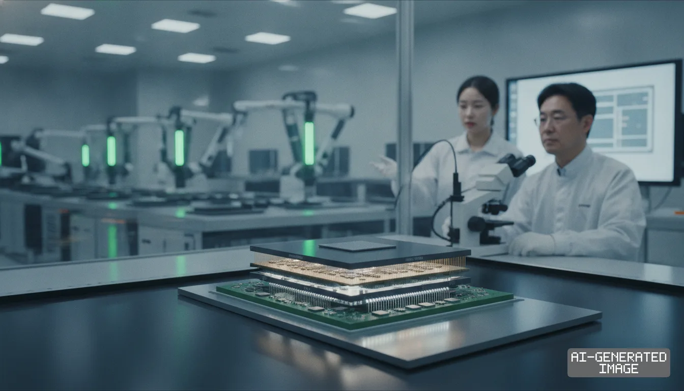
Hyperscale cloud customers adjusted purchase orders with SK hynix on Oct. 31, 2026, downgrading advanced high-bandwidth memory specifications from 12-layer to eight-layer stacks to accelerate delivery schedules.
The change allows server operators to bypass severe packaging queues for 12-layer components. SK hynix, which controls more than 50% of the global high-bandwidth memory market, confirmed the pattern during its quarterly investor briefing.
Customer purchase requests currently exceed the chipmaker's available output by more than two times. That supply gap has forced data center operators to prioritize component delivery speed over maximum memory density per server socket.
Switching from a 12-layer stack to an eight-layer unit yields about 50% more finished memory cubes from identical DRAM wafer inputs. That volume expansion shortens wait times for cloud companies racing to deploy artificial intelligence clusters.
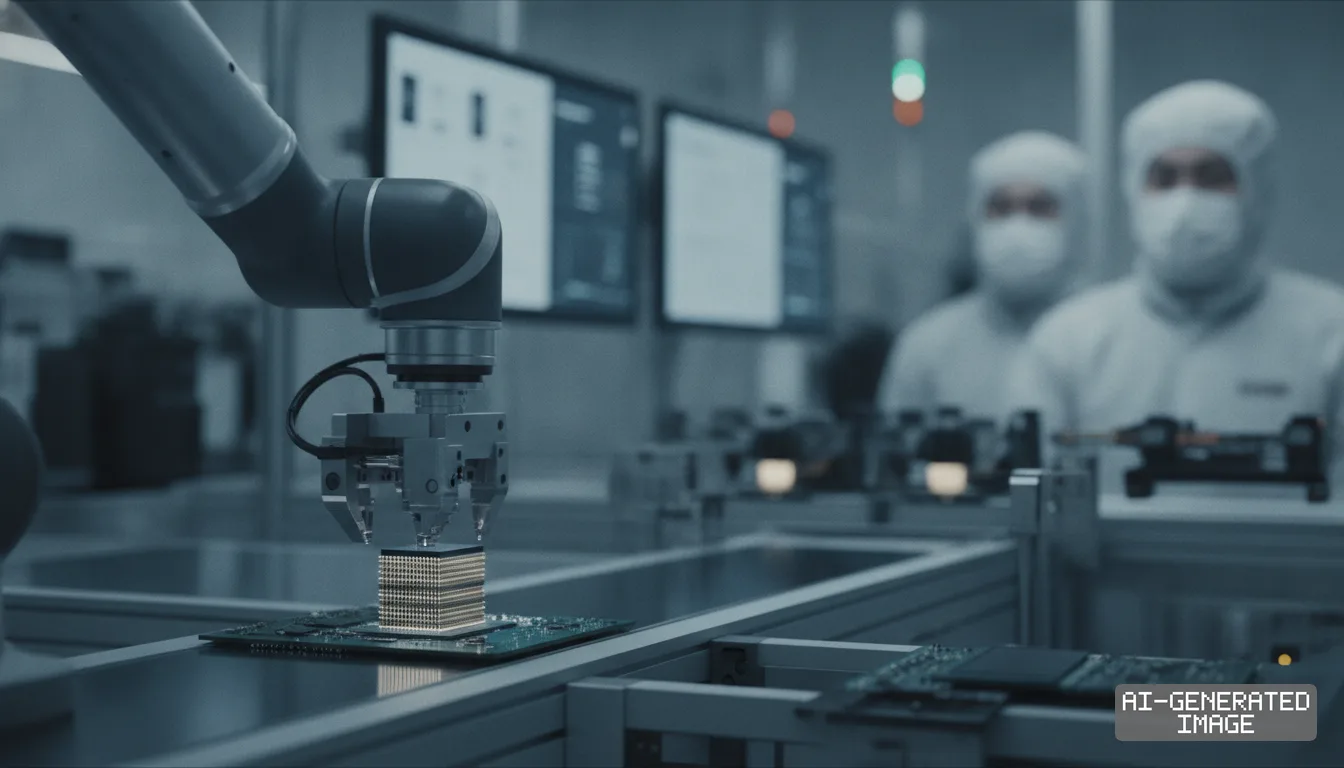
The trade-off shifts manufacturing overhead into back-end operations. Because every high-bandwidth memory cube requires a dedicated logic base die, producing 50% more cubes increases total base-die consumption and multiplies bonding steps.
Those extra assembly requirements add packaging unit costs for system builders. Even with those additions, enterprise operators accept the penalty to secure finished accelerators before competitive commercial deployment windows lapse.
TrendForce reported on Oct. 16 that yield penalties and thermal constraints on 12-layer stacks are driving customers back toward eight-layer configurations. Structural thickness limits in server chassis make heat dissipation significantly more difficult at 12 layers.
Wafer thinning remains the primary technical obstacle in high-stack assembly. Packaging 12 DRAM dies within standardized height envelopes requires grinding silicon wafers down to roughly 50 micrometers, raising micro-crack rates during thermal compression bonding.
Eight-layer stacks utilize thicker dies that sustain higher manufacturing yields. Chipmakers achieve faster throughput on these mature lines because bonding steps drop by a third compared to 12-layer alternatives.
Nvidia takes more than 50% of global high-bandwidth memory output for its data center graphic processors. The company remains highly exposed to advanced packaging throughput at contract fabrication and packaging lines run by Taiwan Semiconductor Manufacturing Company.
Advanced packaging lines running chip-on-wafer-on-substrate technology remain fully booked across East Asia. Stacking fewer memory dies per cube speeds up delivery of finished computing boards to server assemblers.
The specification downgrade also alters wafer allocation across memory fabrication lines. SK hynix must run additional logic interface wafers through foundries to support the larger absolute count of finished memory cubes.
SK hynix said customer orders have already booked its entire high-bandwidth memory capacity through 2029. The supplier reported that memory shortages across enterprise server channels will likely persist through 2030.
The supplier posted record third-quarter operating profit of 83.33 trillion won ($60.4 billion), achieving an operating margin of 80%. High-bandwidth memory and enterprise solid-state drives accounted for the bulk of that margin expansion.
Despite the profitability, capital expenditure plans remain disciplined. SK hynix executives said during the call that production lines will prioritize confirmed long-term supply agreements over speculative cleanroom additions.
The shift illustrates how data center procurement has evolved in 2026. Hyperscalers no longer demand maximum hardware specifications if those components carry multi-quarter delivery delays that stall data center energization.
System architects compensate for lower per-stack density through software clustering and expanded board footprints. By linking more eight-layer accelerator boards together, operators match the raw memory capacity of 12-layer clusters.
That architectural adjustment transfers cost from the memory supplier to data center real estate and electrical infrastructure. Operators require additional rack space and power distribution units to operate the larger physical fleets.
Packaging material suppliers face revised delivery schedules following the customer adjustments. Demand for specialized non-conductive film and liquid epoxy molding compounds is shifting toward form factors tailored to eight-layer dimensions.
Equipment makers supplying high-precision thermocompression bonders see installation schedules adjust as well. Toolmakers must balance deliveries between legacy eight-die bonding systems and advanced fluxless bonding lines designed for next-generation products.
Memory pricing structures reflect the supply imbalance. Average selling prices for DRAM rose in the high-20% range during the third quarter, supported by sustained premiums on high-bandwidth modules.
SK hynix noted that total bit shipments remain insulated from the layer reduction. While individual cubes carry fewer gigabytes, the corresponding 50% increase in finished units preserves aggregate wafer throughput.
The revised purchase agreements take operational effect across system assembly lines on Nov. 15, 2026. Memory modules produced under the adjusted specifications will reach server assembly facilities before the close of the fourth quarter.
SK hynix has not named the specific cloud customers executing the 8-layer downgrades due to non-disclosure agreements, and the company has not published contract-level delivery schedules.
The manufacturer is scheduled to review fourth-quarter delivery volumes and commercial shipments of next-generation HBM4 modules with customer procurement desks in January 2027.
Impact map
How this development propagates across the region and out to global buyers.
| Event | Korea | China | Japan | Global impact |
|---|---|---|---|---|
| HBM stack downgrade | SK hynix gains 50% more cube output per wafer run | domestic server builders face extended memory lead times | materials suppliers shift film specifications to 8-layer formats | Nvidia and hyperscalers accelerate server delivery dates |
In this story
Related briefings
- GlobalFoundries signs $2 billion TSMC chip interposer deal Also on Nvidia, SK hynix, Cost Structure
- SK hynix honors Onto Innovation for advanced HBM inspection Also on Nvidia, SK hynix, Cost Structure
- GlobalFoundries signs $2B TSMC packaging deal for AI chips Also on Nvidia, SK hynix, Cost Structure
- Samsung and SK hynix deploy cooling packaging on HBM4E chips Also on Nvidia, SK hynix, Cost Structure
Sources
Reporting
Confidence: medium — how we grade this
The documents behind this briefing are linked above. East Asia Brief produces its English text with AI assistance under human editorial review, and does not translate or republish other outlets' articles. See our methodology and AI policy. Spotted an error? Tell us.
The Morning Brief
What changed in Korean, Chinese and Japanese industry overnight — and what it means for your supply chain. One email, weekday mornings, US time. Free.
The Morning Brief is in preparation. Leave your address and we will write to you once — when the first issue is ready. Nothing before that.