Samsung Wins 2nm Cloud AI Chip Deal With Taiwan's Faraday
The multi-million-dollar ASIC project shifts an American hyperscaler from a 4nm baseline to Gate-All-Around silicon, with non-recurring engineering revenue starting in 2027.
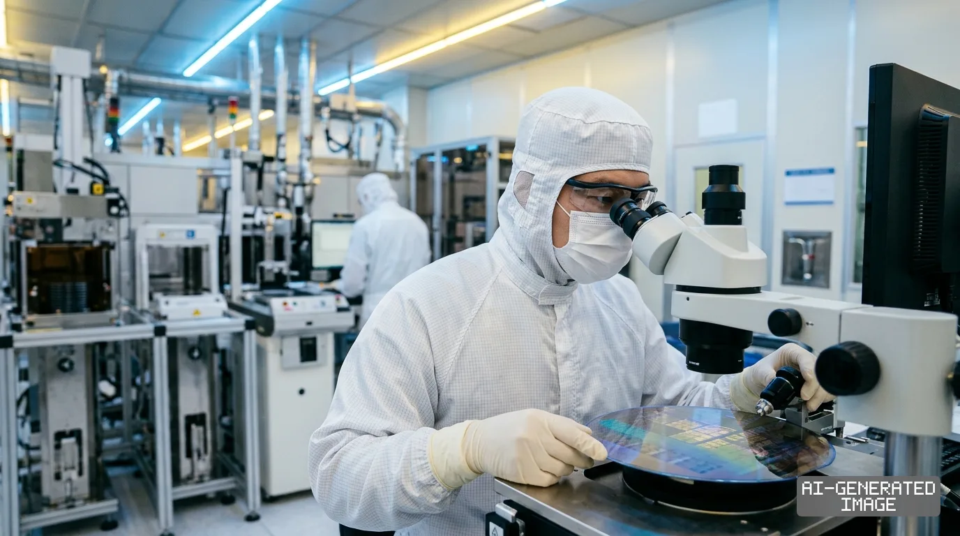
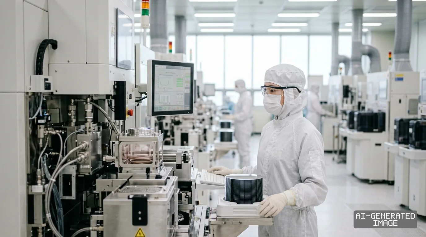
Samsung Electronics secured a manufacturing order Nov. 3, 2026, to fabricate 2-nanometer cloud artificial intelligence chips for an American hyperscaler through Taiwanese design specialist Faraday Technology.
The agreement represents the largest non-recurring engineering contract in Faraday's history, valued in the tens of millions of dollars. Faraday posted NT$3.664 billion ($112.9 million) in total revenue last quarter, with engineering fees accounting for NT$309 million ($9.5 million).
The unnamed American customer initially planned to manufacture the application-specific integrated circuit on a 4-nanometer node. The buyer switched to Samsung's 2-nanometer Gate-All-Around process after reevaluating system energy efficiency, compute density and processor operational lifecycles.
The custom accelerator vertically stacks high-performance logic with specialized three-dimensional dynamic random-access memory using hybrid bonding — a packaging method fusing copper contacts directly without intermediate solder bumps. The architecture supports PCIe Gen6 interconnects and 64-bit floating-point computing.
Faraday serves as the primary design solution partner, managing the physical translation of the client's proprietary neural processing architecture. The Taiwanese engineering house adapts high-level chip schematics into verified physical layouts compliant with Samsung's foundry design rules.
The multi-million-dollar commission marks a major structural shift for Faraday. Mass production of legacy silicon generated 79% of Faraday's consolidated revenue last quarter, while high-margin design engineering services contributed just 8.4% of total top-line receipts.
Revenue recognition for Faraday's non-recurring engineering fees will begin in the first half of 2027, company executives said during an investor briefing. That payment schedule points to physical mask tape-out and silicon prototype verification taking place through late 2027.
For Samsung Foundry, the contract establishes an anchor commercial reference customer for its second-generation Gate-All-Around production platform, branded SF2. Landing high-performance cloud silicon provides outside validation for the company's leading-edge manufacturing roadmap.
Samsung became the first commercial foundry to transition from conventional FinFET transistors to Gate-All-Around nanosheets at the 3-nanometer threshold in 2022. The 2-nanometer node refines nanosheet channel geometry, delivering higher drive current with lower parasitic capacitance.
The production win creates an opening in an advanced cloud accelerator market dominated by Taiwan Semiconductor Manufacturing Co. TSMC manufactures more than 60% of worldwide foundry wafers and fabricates the vast majority of commercial hyperscale AI processors.
Capacity allocations at TSMC's most advanced fabrication facilities and chip-on-wafer packaging lines have remained tight for two consecutive years. Hyperscalers have increasingly sought dual-sourcing options to prevent hardware delivery bottlenecks across multi-gigawatt data center expansion programs.
The contract also establishes a operational foothold for Samsung inside Taiwan's semiconductor engineering community. Faraday historically functioned as the dedicated design services arm of United Microelectronics Corp., concentrating primarily on mature planar nodes.
Samsung has courted Asian design service houses to build out its Samsung Advanced Foundry Ecosystem and rival TSMC's Open Innovation Platform. Enlisting established Taiwanese design firms allows Samsung to solicit international fabless clients without handling custom frontend layouts internally.
The cloud processor relies heavily on advanced packaging integration to overcome bandwidth limits between memory and arithmetic logic. Stacking custom DRAM directly onto the compute die eliminates external wiring delays, accelerating large language model matrix calculations.
Global cloud providers have accelerated internal silicon programs to curb purchases of merchant graphics processors costing upwards of $30,000 per unit. Proprietary chips allow platform operators to tailor memory bandwidth to specific neural network algorithms.
Leading-edge 2-nanometer processed wafers command industry contract prices exceeding $25,000 each. Moving from 4-nanometer to 2-nanometer significantly increases frontend photomask tooling expenses, but lowers long-term electricity consumption across thousands of operational server racks.
Samsung will fabricate the 2-nanometer wafers across its domestic production lines in Giheung and Hwaseong, South Korea. The company has also installed high-numerical-aperture extreme ultraviolet lithography systems at its Pyeongtaek complex to prepare for mass node transitions.
Samsung executives projected during third-quarter earnings discussions that manufacturing operations for nodes at 8-nanometer and below will exceed 100% capacity utilization next year. Company management noted that commercial orders for 2-nanometer wafer processing doubled during 2026.
The hyperscaler's choice to bypass 4-nanometer silicon highlights the shifting economics of enterprise artificial intelligence hardware. Cloud operators now prioritize multidecade processor longevity over near-term engineering cost savings when outfitting core data centers.
For Faraday, executing a 2-nanometer physical design utilizing hybrid bonding represents the technically most complex engagement since the firm's founding in 1993. The company is assigning specialized engineering teams across design centers in Hsinchu, the United States and Vietnam.
The project signals rising competitive pressure for rival Taiwanese ASIC specialists such as Alchip Technologies and Global Unichip Corp. Access to alternative leading-edge foundry capacity allows design partners to guarantee wafer delivery schedules to major cloud clients.
Samsung continues to realign capital allocation within its contract manufacturing division toward profitable leading-edge nodes. The company confirmed plans to phase out its legacy eight-inch wafer fabrication lines by 2030 to concentrate resources on sub-3-nanometer architectures.
Revenue recognition for Faraday begins in the first half of 2027, when design engineers complete the initial physical placement and routing verification milestones.
The disclosures do not state the identity of the American cloud customer, and Samsung has not published the total wafer production contract value or unit volume.
Impact map
How this development propagates across the region and out to global buyers.
| Event | Korea | China | Japan | Global impact |
|---|---|---|---|---|
| 2nm Cloud AI ASIC Order | Samsung Foundry lands anchor 2nm GAA cloud reference customer | Faraday secures record tens of millions in NRE fees, expanding beyond UMC | Toolmakers see EUV and hybrid bonding equipment procurement firm for 2027 | US hyperscaler bypasses 4nm to diversify cloud compute supply away from TSMC |
In this story
- Companies
- Samsung ElectronicsFaraday Technology
- Tickers
- 005930.KS3035.TW
- Exposed
- TSMCUnited Microelectronics Corp.
- Impact
- Order BookCapexSupply Chain
Related briefings
- TSMC captures 72.5% foundry share as gap with Samsung widens Also on United Microelectronics Corp., Samsung Electronics
- TSMC raises foundry prices for fabless clients by up to 10% in 2027 Also on United Microelectronics Corp., Samsung Electronics
- TSMC plans to lift wafer foundry prices by 3% to 6% from 2027 Also on United Microelectronics Corp., Samsung Electronics
- TSMC and Japanese Auto Suppliers Scale 28nm BCD Power Chip Production Also on United Microelectronics Corp., Order Book
Sources
Reporting
Confidence: medium — how we grade this
The documents behind this briefing are linked above. East Asia Brief produces its English text with AI assistance under human editorial review, and does not translate or republish other outlets' articles. See our methodology and AI policy. Spotted an error? Tell us.
The Morning Brief
What changed in Korean, Chinese and Japanese industry overnight — and what it means for your supply chain. One email, weekday mornings, US time. Free.
The Morning Brief is in preparation. Leave your address and we will write to you once — when the first issue is ready. Nothing before that.