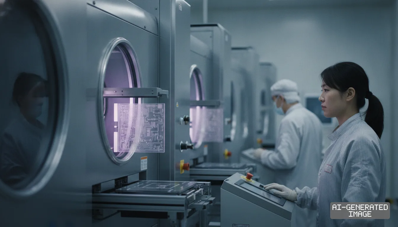
TSMC raises 2nm wafer target to 120,000 units as orders surge
The foundry lifted internal production goals by pulling forward capacity additions after Apple, Nvidia and three other anchor clients expanded bookings by up to 20%.
Taiwan Semiconductor Manufacturing Company lifted its internal 2-nanometer production goal to 120,000 wafers per month on Sept. 28, 2026, pulling forward factory schedules following aggressive advance orders from key customers.
The revised monthly target advances a production threshold originally planned for 2027. It exceeds earlier industry projections of 90,000 to 100,000 monthly wafers by at least 20,000 units.
Five major customers — Apple, Nvidia, Advanced Micro Devices, Qualcomm and MediaTek — increased their 2-nanometer wafer reservation requests by 10% to 20%, according to commercial supply-chain reports.
The upward revision follows operational briefings conducted on Sept. 14, 2026. TSMC had informed equipment partners that 2-nanometer capacity would reach 110,000 wafers monthly by mid-2027.
That earlier projection called for 90,000 monthly wafers by the end of 2026. The mid-2027 operational plan also scheduled 3-nanometer line throughput to expand to 210,000 wafers per month.
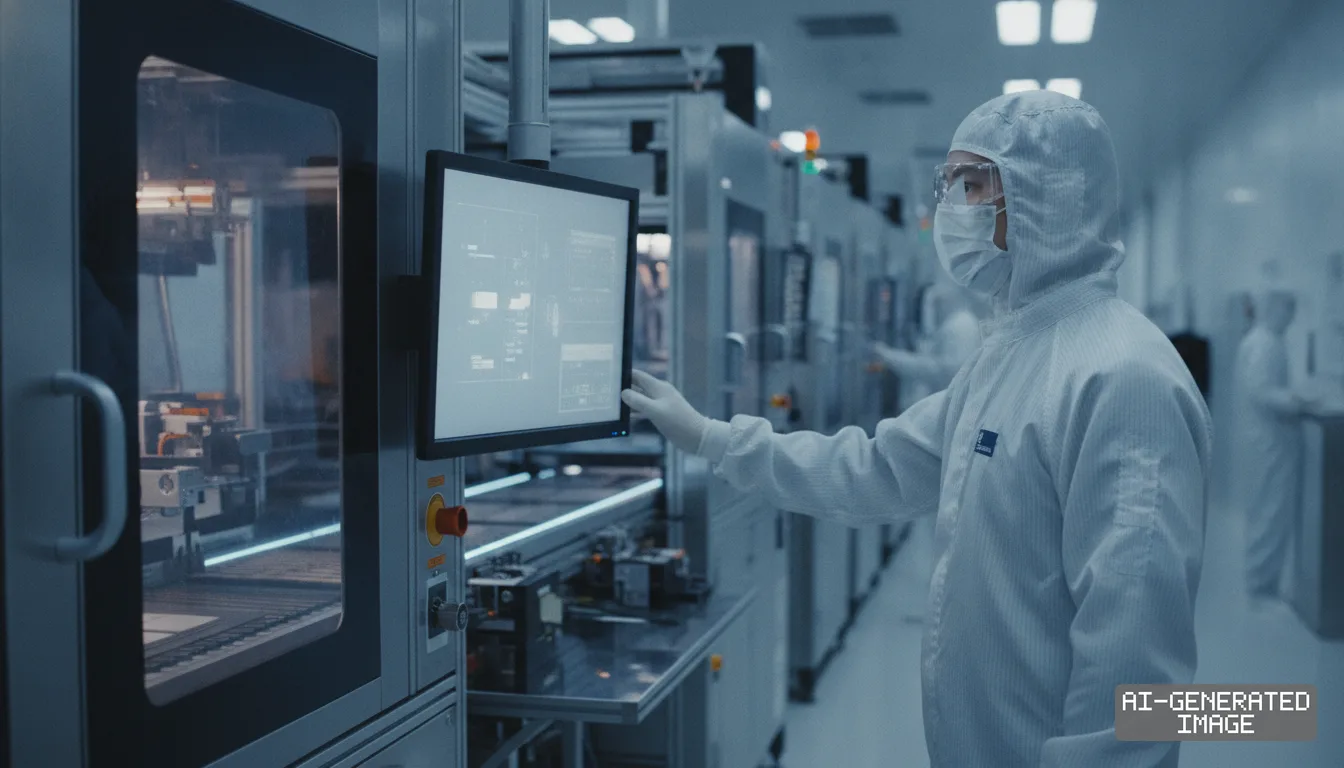
The accelerated schedule requires tool vendors to expedite deliveries of extreme ultraviolet lithography systems. Facilities teams are advancing cleanroom certification to support the higher monthly run rate.
Cloud service providers and processor designers are driving the aggressive order patterns. Artificial intelligence model developers are shortening hardware refresh intervals, generating immediate demand for higher transistor density.
The 2-nanometer process node, designated N2, represents TSMC's commercial transition to nanosheet transistors. The architecture surrounds the conducting silicon channel on all four sides to minimize electrical leakage.
The gate-all-around design delivers full-node improvements in computing speed and operational efficiency over existing FinFET structures. TSMC is applying the architecture across both smartphone and high-performance computing platforms.
Smartphone vendors require initial production runs for flagship mobile chipsets scheduled for market release in late 2026. Server processor vendors are securing wafer starts for next-generation computing accelerators.
Capital spending plans support the accelerated factory expansion. In July 2026, TSMC officially raised its full-year capital expenditure forecast to a range of $60 billion to $64 billion.
Advanced logic process technologies will absorb between 70% and 80% of that full-year capital expenditure budget, TSMC management said during the company's second-quarter earnings conference call.
The allocated capital funds extreme ultraviolet lithography machines, chemical vapor deposition systems and automated wafer transportation systems across multiple leading-edge fabrication sites in western Taiwan.
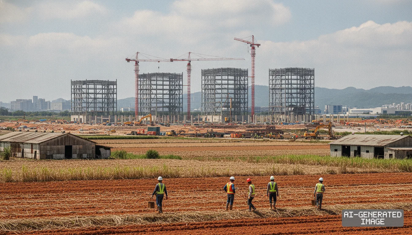
TSMC is simultaneously preparing five separate fabrication lines to handle the expanded 2-nanometer production volumes. Construction and cleanroom installation work are proceeding simultaneously at two distinct industrial clusters.
At the North America Technology Symposium on April 22, 2026, Senior Vice President and Co-Chief Operating Officer Y.P. Yong-Ching Hou detailed the multi-site 2-nanometer manufacturing ramp.
The company is installing two manufacturing modules at the Hsinchu Science Park, Hou said. Three additional 2-nanometer fabrication lines are under active deployment at the Kaohsiung industrial science park.
First-year wafer output for the 2-nanometer node will exceed first-year 3-nanometer volumes by 45%, Hou said. The 3-nanometer process completed its initial production year in 2023.
TSMC projected a compound annual growth rate of 70% for 2-nanometer wafer shipments from 2026 through 2028, according to official presentation materials distributed during the symposium.
The rapid expansion of TSMC's 2-nanometer line capacity limits market opportunities for rival contract foundries. Samsung Electronics has marketed its proprietary gate-all-around fabrication services to top-tier fabless semiconductor designers.
Samsung introduced gate-all-around nanosheet transistors at its 3-nanometer node in 2022. Commercial adoption among premier international artificial intelligence hardware vendors has nevertheless remained concentrated at TSMC.
Securing anchor allocation contracts across Apple, Nvidia and AMD absorbs leading-edge manufacturing capacity through 2027. That dynamic restricts the market window for alternative foundries seeking volume commitments.
Customer commitment to TSMC is reinforced by advanced packaging integrations. Leading artificial intelligence processors combine 2-nanometer logic dies with high-bandwidth memory using TSMC's Chip-on-Wafer-on-Substrate packaging platforms.
TSMC operates its advanced packaging facilities in geographic proximity to its domestic fabrication lines in Taiwan. This geographic clustering lowers logistical transit risks for complex multi-chip semiconductor assemblies.
Domestic fabrication facilities in Hsinchu and Kaohsiung will maintain exclusive commercial responsibility for 2-nanometer volume wafer production through the end of 2027, according to corporate disclosures.
Overseas manufacturing sites will integrate the technology at a later stage. TSMC plans to introduce 2-nanometer production at its second Arizona fabrication plant starting in 2028.
Taiwan Semiconductor Manufacturing Company has not published a formal regulatory filing confirming the 120,000-wafer monthly target, and corporate representatives declined to verify individual customer capacity booking figures.
Commercial volume production milestones and potential capital expenditure adjustments will be formally reviewed during TSMC's regular quarterly investor earnings conference scheduled for Oct. 15, 2026.
Impact map
How this development propagates across the region and out to global buyers.
| Event | Korea | China | Japan | Global impact |
|---|---|---|---|---|
| 2nm wafer capacity expansion | Samsung Foundry faces reduced customer acquisition window across tier-one fabless designers | Domestic AI developers remain blocked from leading-edge GAA foundry allocations | Equipment vendors accelerate deliveries of advanced lithography and track systems | Leading-edge logic wafer supply tightens as Apple and Nvidia secure initial production runs |
In this story
Track every Subsidies development →
Related briefings
- Qualcomm keeps TSMC for 2nm processors, shutting out Samsung Foundry Also on MediaTek, Qualcomm, Apple
- MediaTek debuts first 2nm mobile AP built on TSMC N2P node Also on MediaTek, Qualcomm, Apple
- Samsung narrows SK hynix HBM lead as HBM4 shipments expand Also on AMD, TSMC, Nvidia
- TSMC plans to lift wafer foundry prices by 3% to 6% from 2027 Also on Qualcomm, Apple, Nvidia
Sources
Primary documents
Reporting
Confidence: high — how we grade this
The documents behind this briefing are linked above. East Asia Brief produces its English text with AI assistance under human editorial review, and does not translate or republish other outlets' articles. See our methodology and AI policy. Spotted an error? Tell us.
The Morning Brief
What changed in Korean, Chinese and Japanese industry overnight — and what it means for your supply chain. One email, weekday mornings, US time. Free.
The Morning Brief is in preparation. Leave your address and we will write to you once — when the first issue is ready. Nothing before that.