Samsung and SK hynix split 2.5 million pyeong Gwangju fab site
Samsung secures 1.2 million pyeong while SK hynix takes 1.0 million pyeong under an 800 trillion won project to build four memory cleanroom lines.
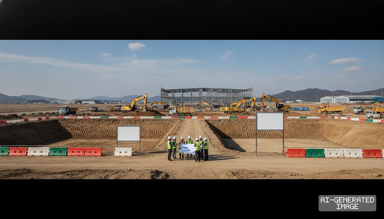
South Korean authorities finalized a dual-track land distribution on Nov. 18, 2026, partitioning the 2.5 million pyeong Gwangju airport site between Samsung Electronics and SK hynix for four memory fabs.
The project outlines a combined capital outlay of 800 trillion won ($580 billion), split evenly at 400 trillion won per producer. Each chipmaker plans two cleanroom production lines on the converted parcel.
Under the framework, Samsung Electronics secures roughly 1.2 million pyeong (3.97 million square meters) in the southern sector. SK hynix takes 1.0 million pyeong in the northern parcel. The remaining 300,000 pyeong is set aside for municipal roads and shared utility terminals.
The development serves as the manufacturing anchor for the Southwestern Semiconductor Cluster, established by the presidential office on July 6, 2026. Planners designed the complex to alleviate acute transmission shortages that stall semiconductor fab construction in Gyeonggi Province.
The Yongin Semiconductor Mega Cluster, located south of Seoul, faces power deficits that exceed 10 gigawatts through 2030. High-voltage transmission lines connecting external plants to Yongin remain delayed by route negotiations across multiple municipalities.
Planners selected Gwangju to link memory production directly with renewable energy networks in South Jeolla Province. The region hosts expansive photovoltaic plants and the upcoming Sinan offshore wind installation. The coastal grid also draws baseload electricity from the Hanbit nuclear power station.
Samsung Electronics had sought northern parcels to secure proximity to KTX GwangjuSongjeong Station and downtown housing quarters. SK hynix contested the same boundary to accelerate engineering groundwork and logistics handling.
Planners assigned the northern parcel to SK hynix after the company pledged accelerated construction timetables. SK hynix also accepted technical adjustments to accommodate local transportation corridors.
Water infrastructure planning is already underway. The municipal utility framework calls for an initial intake of 150,000 metric tons of industrial water daily, piped from the Juam and Dongbok reservoirs.
Power authorities plan a dedicated 3.1-gigawatt substation branch connecting Gwangju to the regional 345-kilovolt transmission network. The circuit will run through a 23-kilometer underground conduit along provincial routes to prevent overhead line disputes.
Samsung Electronics maintains approximately 60% of its global DRAM output at Pyeongtaek and Hwaseong. The 400 trillion won envelope in Gwangju expands its domestic cleanroom footprint by roughly 30% over the coming decade.
SK hynix concentrates its wafer processing in Icheon and Cheongju while investing 122 trillion won in Yongin. The 400 trillion won Gwangju commitment represents an additional long-range production pole for high-bandwidth memory (HBM) stacking.
Advanced packaging and wafer-level testing require steady power supplies that municipal grids in the capital zone cannot guarantee before 2032. Fab operators calculate that electricity curtailment risks in Gyeonggi outweigh relocation expenses to southern provinces.
The Ministry of Trade, Industry and Energy has not published an official gazette confirming the internal plot division, and neither chipmaker has issued an exchange filing detailing the capital expenditure schedule.
Government coordinators plan to sign formal investment covenants with both companies by Dec. 31, 2026. Public developer Korea Land & Housing Corp. intends to start site grading on an initial 630,000-pyeong section in 2027, aiming for commercial chip production by June 2030.
Impact map
How this development propagates across the region and out to global buyers.
| Event | Korea | China | Japan | Global impact |
|---|---|---|---|---|
| Gwangju airport semiconductor fab site allocation | Samsung takes 1.2M pyeong south and SK hynix takes 1.0M pyeong north for 800T won memory hub | CXMT faces expanded long-term Korean memory capacity outside vulnerable capital grid | Tokyo Electron and Screen Holdings position service hubs for 2030 fab lines | Memory supply diversification accelerates away from single-point transmission risks in Seoul ring |
In this story
- Companies
- Samsung ElectronicsSK hynix
- Tickers
- 005930.KS000660.KS
- Policy
- Subsidies
- Impact
- CapexSupply Chain
Track every Subsidies development →
Related briefings
- CXMT lifts DRAM market share to 10% in legacy memory offensive Also on SK hynix, Samsung Electronics, Subsidies
- SK hynix pulls forward 600 trillion won Yongin fab finish to 2033 Also on SK hynix, Samsung Electronics, Subsidies
- Samsung begins $104B regional push with Onyang packaging fab Also on SK hynix, Samsung Electronics, Subsidies
- Samsung breaks ground on $33B advanced packaging fab in Asan Also on SK hynix, Samsung Electronics, Subsidies
Sources
Reporting
Confidence: medium — how we grade this
The documents behind this briefing are linked above. East Asia Brief produces its English text with AI assistance under human editorial review, and does not translate or republish other outlets' articles. See our methodology and AI policy. Spotted an error? Tell us.
The Morning Brief
What changed in Korean, Chinese and Japanese industry overnight — and what it means for your supply chain. One email, weekday mornings, US time. Free.
The Morning Brief is in preparation. Leave your address and we will write to you once — when the first issue is ready. Nothing before that.