Rapidus holds 2nm chip timeline as 17 partners join network
The Japanese venture keeps its 2027 mass-production goal while enlisting Cadence and Synopsys to lower design barriers against foundry leaders TSMC and Samsung.
Rapidus Corporation stood on Oct. 9, 2026 by its 2027 mass-production timetable for 2-nanometer logic chips, keeping trial manufacturing parameters intact while rolling out its new customer design network.
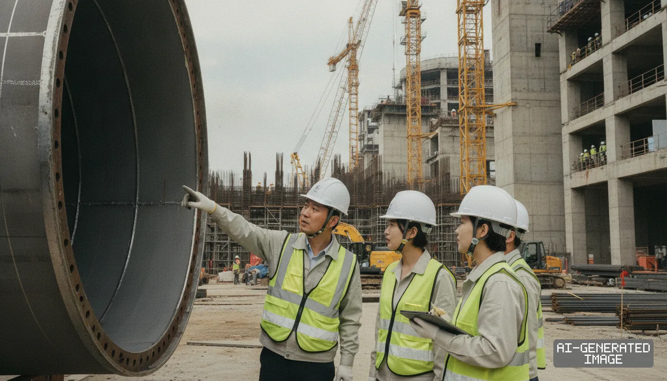
The venture operates its pilot line at the IIM-1 facility in Chitose, Hokkaido. Japan's Ministry of Economy, Trade and Industry has committed up to 1.72 trillion yen ($11.5 billion) in subsidies to fund the project through state research body NEDO.
The state subsidies cover roughly a third of the estimated 5 trillion yen ($33.5 billion) required for commercial ramp-up. Rapidus relies on gate-all-around architecture — where transistor gates surround silicon channels on all sides — to reach 2 nanometers.
Securing manufacturing yields at 2 nanometers does not automatically guarantee commercial adoption. Fabless chip designers must adapt complex architectures to new process design kits, automated toolsets and packaging standards before committing to wafer runs, analysts said.
To address that friction, Rapidus unveiled the Rapidus Collaborative Open Rapid Ecosystem on Oct. 5. The framework brings 17 external design and service companies into a dedicated group named Design Solution Associates to assist early-stage customer chip planning.
Cadence Design Systems and Synopsys represent the core software partners in the alliance. The two American firms control more than 70% of the global electronic design automation market, providing the simulation flows necessary to verify physical layouts before fabrication.
Cadence integrated its InnoStack artificial intelligence engine with Rapidus in July. The partnership targets a 2X acceleration in design turnaround time to help smaller design teams build custom chips, Cadence said.
Japanese manufacturing suppliers Dai Nippon Printing and TOPPAN also joined the design group. The two suppliers produce roughly 80% of merchant photomasks in Japan, providing critical reticle alignment and packaging support for the Hokkaido fab lines.
Global IT service vendors including Infosys, Wipro and HCL Technologies joined the roster to provide front-end engineering staff. The three firms employ hundreds of thousands of engineers, helping bridge regional semiconductor engineering shortages across Asia.
The Rapidus push directly touches the regional foundry landscape in East Asia. Taiwan Semiconductor Manufacturing Company currently holds more than 90% of global contract capacity for chips made on sub-5-nanometer nodes, concentrating geographic supply risk in Taiwan.
TSMC began pilot runs on its own 2-nanometer process in 2025 and plans high-volume commercial production in Taiwan during 2026. The Taiwanese company also operates advanced packaging facilities that dominate artificial intelligence accelerator output.
Samsung Electronics maintains roughly 11% of the worldwide foundry market and is marketing its second-generation gate-all-around node to high-performance computing customers. The South Korean manufacturer has targeted commercial 2-nanometer deployments to draw clients away from TSMC.
Surging demand for artificial intelligence hardware has led technology firms to look beyond single suppliers. U.S. processor designer Tenstorrent signed a development partnership with Rapidus in 2024 to design edge artificial intelligence accelerators on the node.
Rapidus developed its core transistor process through an alliance with International Business Machines Corporation. The Japanese chipmaker dispatched more than 150 engineers to IBM's Albany NanoTech Complex in New York to establish manufacturing baseline parameters.
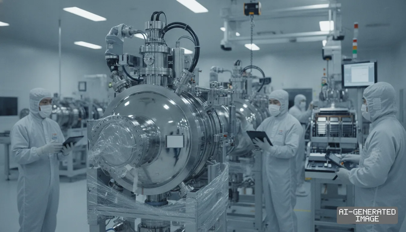
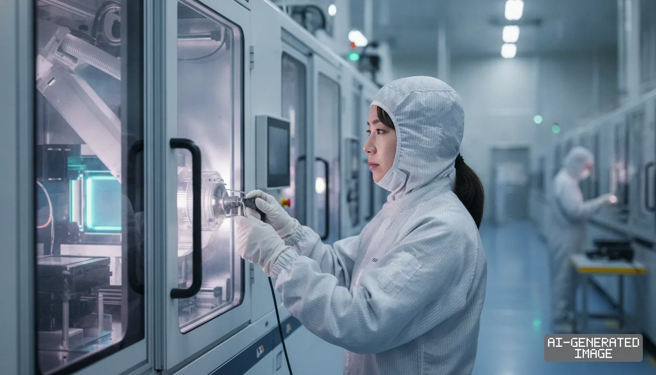
Technicians installed Japan's first production-grade extreme ultraviolet lithography system at Chitose in late 2024. Rapidus activated the cleanroom in April 2025 to run test wafers through trial gates and measure basic transistor characteristics, the company said.
Advanced packaging represents the second leg of the Chitose manufacturing strategy. Modern artificial intelligence accelerators rely on multi-chiplet packaging, which links multiple semiconductor dies on silicon interposers to maximize data transfer speeds and energy efficiency.
Rapidus is developing dedicated packaging facilities under Rapidus Chiplet Solutions adjacent to IIM-1. The company leases 9,000 square meters of cleanroom space from Seiko Epson Corporation in Chitose to develop 2.5-dimensional and three-dimensional stacking lines.
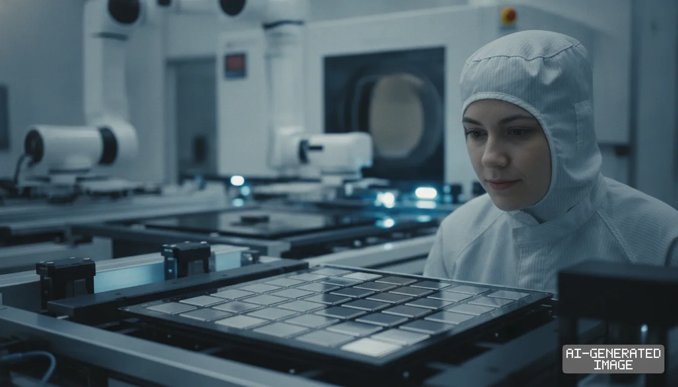
The packaging facility is testing 600-millimeter square redistribution layer panels. Using large square panels rather than standard 300-millimeter circular wafers can significantly increase the usable area for interposers that connect logic dies to high-bandwidth memory.
Private funding remains a critical hurdle for the project as mass production nears. A syndicate of Japanese lenders and corporate backers invested 267.6 billion yen ($1.7 billion) in equity in early 2026, lifting total paid-in capital.
Rapidus plans to start equipment installations at its Chitose back-end packaging facility in April 2027 ahead of volume commercial output targeted for late 2027, according to company schedules published by trade authorities.
The company and trade officials have not published revised trial manufacturing targets as of Oct. 9, and Rapidus has not disclosed binding commercial production contracts or confirmed volume customer tape-outs.
Japan's New Energy and Industrial Technology Development Organization approved the current operating budget in July, keeping project monitoring under the existing Post-5G information infrastructure framework through fiscal 2026.
Impact map
How this development propagates across the region and out to global buyers.
| Event | Korea | China | Japan | Global impact |
|---|---|---|---|---|
| Rapidus 2nm design ecosystem rollout | Samsung faces 2nm GAA alternative for fabless AI chip orders | Excluded from GAA design tooling partnerships under export controls | DNP and TOPPAN secure domestic merchant photomask integration for 2nm | TSMC maintains >90% advanced node share as customers trial secondary sources |
In this story
- Companies
- Rapidus
- Exposed
- Cadence Design SystemsSynopsysTSMCSamsung ElectronicsDai Nippon PrintingTOPPAN
- Policy
- SubsidiesEconomic Security
- Impact
- Supply ChainCapexCost Structure
Track every Subsidies development → Track every Economic Security development →
Related briefings
- Rapidus forms 17-firm design alliance to back 2nm chip ramp Also on Cadence Design Systems, Synopsys, Dai Nippon Printing
- Synopsys certifies TSMC A14 EDA flows and tapes out 64G UCIe Also on Cadence Design Systems, Synopsys, TSMC
- Synopsys expands TSMC pact with agentic AI chip design tools for A14 Also on Cadence Design Systems, Synopsys
- Rapidus begins trial runs on 2nm pilot line in Hokkaido ahead of 2027 target Also on Dai Nippon Printing, Rapidus, TSMC
Sources
Primary documents
Reporting
Confidence: high — how we grade this
The documents behind this briefing are linked above. East Asia Brief produces its English text with AI assistance under human editorial review, and does not translate or republish other outlets' articles. See our methodology and AI policy. Spotted an error? Tell us.
The Morning Brief
What changed in Korean, Chinese and Japanese industry overnight — and what it means for your supply chain. One email, weekday mornings, US time. Free.
The Morning Brief is in preparation. Leave your address and we will write to you once — when the first issue is ready. Nothing before that.