Rapidus begins trial runs on 2nm pilot line in Hokkaido ahead of 2027 target
Japan's state-backed foundry venture powers up cleanroom tools in Chitose, testing gate-all-around transistor yields with domestic equipment makers.
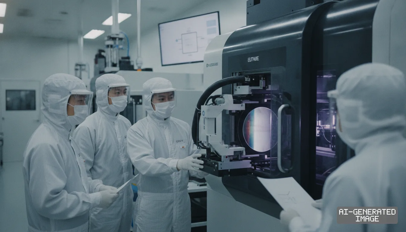
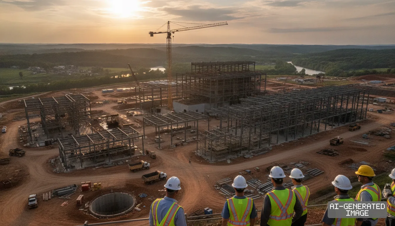
Rapidus Corporation has started pilot operations on its 2-nanometer logic semiconductor line at its Innovative Integration for Manufacturing facility in Chitose, Hokkaido, initiating test wafer processing aimed at mass production in 2027.
The state-backed venture, established in 2022 by eight Japanese corporations alongside government capital, is attempting to compress the standard five-year leading-edge foundry ramp into a 36-month timeline. The pilot run marks the operational debut of extreme ultraviolet lithography systems installed at the site earlier this year, focusing on baseline defect density calibration and transistor formation using gate-all-around architectures. Japan's Ministry of Economy, Trade and Industry has allocated up to 920 billion yen ($6.3 billion) in direct subsidies to Rapidus to date, positioning the venture as the anchor of the country's economic security framework for advanced logic supply.
For global chip designers and institutional investors monitoring foundry concentration risks in Taiwan, the Hokkaido trial run represents the first physical test of whether an entrant without prior fab operations can run a commercial 2nm line. The project relies on gate-all-around nanosheet architecture licensed from IBM Corporation's Albany NanoTech Complex, combined with advanced packaging processes designed to run concurrently with front-end wafer fabrication.
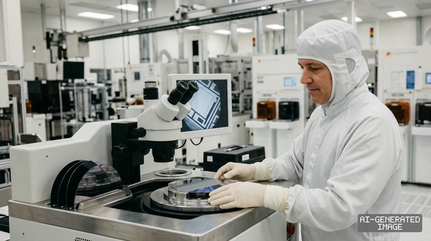
The initial pilot line, designated IIM-1, has installed ASML High-NA and standard 0.33 numerical aperture EUV lithography machines, alongside dry etching, atomic layer deposition, and chemical mechanical planarization equipment supplied by Tokyo Electron, Canon, and Screen Holdings. Engineers at the facility began cycling 300-millimeter blanket test wafers through the lithography cluster during the first week of August, measuring overlay accuracy and critical dimension uniformity across the exposure field.
The primary technical hurdle for Rapidus centers on transitioning IBM's laboratory-scale process flow into a continuous, high-yield manufacturing cycle. In conventional foundries such as Taiwan Semiconductor Manufacturing Company and Samsung Electronics, node transitions build on decades of accumulated inline yield management data, specialized recipe libraries, and established maintenance cycles. Rapidus is attempting to bypass intermediate fin field-effect transistor nodes entirely, moving directly from legacy 45-nanometer domestic capability to 2nm nanosheet technology.
To bridge this operational gap, Rapidus dispatched more than 100 engineers to the Albany NanoTech Complex in New York for process integration training over an 18-month deployment. Those personnel have returned to Chitose to lead tool qualification alongside field engineers from ASML and Tokyo Electron. The immediate objective of the pilot phase is achieving stable baseline electrical characteristics on single-transistor test vehicles before introducing multi-layer metallization routing in early 2027.
The commercial feasibility of the Hokkaido fab depends heavily on its backend packaging integration model, known as Rapid and Unified Manufacturing Services. Unlike traditional contract foundries that treat wafer fabrication and packaging as separated operational phases handled across different facilities or third-party assembly houses, Rapidus is co-locating front-end 2nm processing with 2.5D and 3D interposer packaging within the Chitose complex.
This packaging strategy ties Rapidus directly to domestic materials and substrate specialists. Dai Nippon Printing and Toppan Holdings are supplying photomasks and advanced redistribution layer interposers, while Resonac Holdings and Ajinomoto Fine-Techno provide mold resins and build-up films engineered for high-density chiplet interconnects. By keeping substrate attachment and wafer-to-wafer hybrid bonding in the same physical cleanroom perimeter, Rapidus claims it can reduce total cycle time for custom application-specific integrated circuits from months to weeks.
Procurement directors at North American fabless semiconductor firms have treated the venture with measured engagement, evaluating test silicon while keeping volume allocations committed to TSMC's N2 and A16 nodes in Hsinchu and Kaohsiung. Rapidus has opened a sales and design support office in Santa Clara, California, targeting artificial intelligence accelerator startups and high-performance computing developers that require low-volume, rapid-turnaround wafer runs rather than smartphone-scale volume.
Securing commercial customer commitments remains constrained by capital requirements. The total capital expenditure needed to bring the Chitose site to full commercial volume of approximately 25,000 wafer starts per month by 2027 is estimated by Japan's Ministry of Economy, Trade and Industry at 5 trillion yen ($34.5 billion). While government grants have covered initial cleanroom construction and pilot tooling, the company must raise roughly 3 trillion yen in private equity, commercial loans, and customer prepayments to fund volume manufacturing equipment clusters.
Japan's major financial institutions, including Mitsubishi UFJ Financial Group, Sumitomo Mitsui Banking Corporation, and the Development Bank of Japan, have linked their long-term debt financing packages to verified pilot yield data and firm customer purchase agreements. The current test runs in Chitose are structured to generate the empirical defect rate metrics required by commercial credit committees before loan syndication closes in mid-2027.
On the domestic policy side, the Japanese Diet is preparing amendments to the Act on Strengthening Semiconductor Industrial Foundations during the upcoming autumn legislative session. The proposed statutory revisions will permit the state-backed Organization for Small & Medium Enterprises and Regional Innovation to guarantee bank loans extended to advanced chip ventures and allow the government to convert its direct capital equipment subsidies into non-voting equity shares in Rapidus.
Tool delivery schedules for the remaining process bays at IIM-1 indicate that secondary chemical vapor deposition clusters and automated wafer transfer tracks will be installed continuously through December 2026, with the first full-mask customer test chip run scheduled for the second quarter of 2027.
Impact map
How this development propagates across the region and out to global buyers.
| Event | Korea | China | Japan | Global impact |
|---|---|---|---|---|
| Rapidus 2nm pilot operations | memory packaging interfaces monitored | advanced logic equipment restrictions persist | domestic equipment and material orders rise | alternative leading-edge foundry source tested |
In this story
- Companies
- RapidusTokyo ElectronResonac HoldingsIBM
- Tickers
- 8035.T4004.TIBM
- Exposed
- TSMCASMLDai Nippon PrintingToppan Holdings
- Policy
- SubsidiesEconomic Security
- Impact
- Supply ChainCapexOrder Book
Track every Subsidies development → Track every Economic Security development →
Related briefings
- Rapidus forms 17-firm design alliance to back 2nm chip ramp Also on IBM, TOPPAN Holdings, Dai Nippon Printing
- Rapidus holds 2nm chip timeline as 17 partners join network Also on Dai Nippon Printing, Rapidus, TSMC
- TOPPAN and Broadcom open Singapore plant for AI substrates Also on TOPPAN Holdings
- Japan Expands CMP Slurry Lines for Backside Power Also on Resonac Holdings, Rapidus, Order Book
Sources
This briefing carries no sources block. It was written from our desks’ working knowledge of the sector rather than from documents retrieved for this piece. Read it as orientation and check any figure you intend to act on — how we source briefings.
This briefing carries no linked sources: it was written from our desks' working knowledge of the sector rather than from documents retrieved for this piece. East Asia Brief publishes no citation it cannot link. Our English text is produced with AI assistance under human editorial review. See our methodology and AI policy. Spotted an error? Tell us.
The Morning Brief
What changed in Korean, Chinese and Japanese industry overnight — and what it means for your supply chain. One email, weekday mornings, US time. Free.
The Morning Brief is in preparation. Leave your address and we will write to you once — when the first issue is ready. Nothing before that.