Rapidus forms 17-firm design alliance to back 2nm chip ramp
The Japanese foundry partnered with Synopsys, Cadence and domestic design houses to build an IP library and reduce client reliance on TSMC ahead of planned 2027 commercial output.
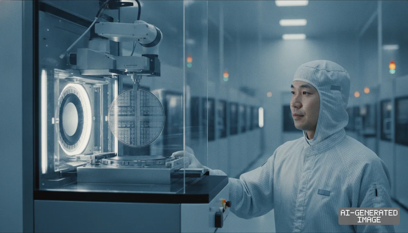
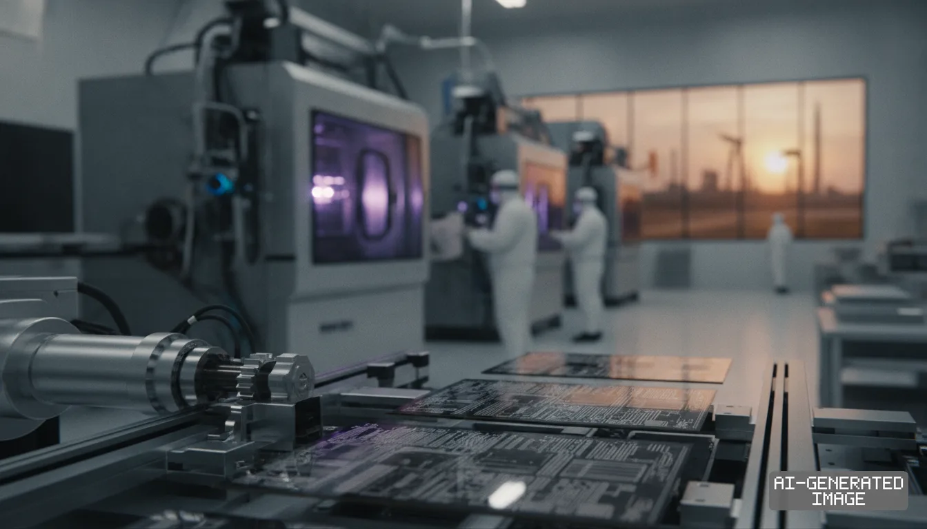
Rapidus formed an alliance with 17 semiconductor design and software companies on Oct. 4, 2026 to support client chip development ahead of scheduled 2-nanometer mass production.
The state-backed venture is building its IIM-1 wafer fabrication facility in Chitose, Hokkaido, supported by 920 billion yen ($6.3 billion) in direct research subsidies approved by the Japanese government.
The new partner network targets global fabless customers who design proprietary chips but rely on contract manufacturers to fabricate silicon wafers, Nikkei reported on Oct. 4.
United States toolmakers Synopsys and Cadence Design Systems headline the design automation tier. Both supply electronic design automation (EDA) software used to map billions of microscopic transistors across silicon wafers.
Cadence integrated its InnoStack artificial intelligence software into the Rapidus Raads design platform in July 2026. The integration aims to deliver up to a 2X reduction in chip design turnaround times.
Toshiba Information Systems and India-based Infosys supply specialized engineering capacity. Their design service teams translate high-level processor architectures into physical circuit layouts ready for lithography tools, the report said.
Dai Nippon Printing and TOPPAN Holdings provide photomask tooling. The two Japanese printing conglomerates manufacture the precision quartz plates that project circuit patterns onto silicon wafers during extreme ultraviolet exposure.
The alliance mirrors the Open Innovation Platform created by Taiwan Semiconductor Manufacturing Co. (TSMC). TSMC controls over 60% of worldwide foundry output, backed by thousands of pre-tested silicon design blocks.
Without certified design rules and layout libraries, prospective chip buyers cannot reroute orders to Rapidus. Developing those interface components requires deep cooperation between the foundry and independent design service providers.
Atsuyoshi Koike, chief executive officer of Rapidus, said the foundry will cut chip manufacturing cycles by roughly two-thirds. The venture uses a single-wafer processing method rather than traditional multi-wafer batch processing lines.
Rapidus verified gate-all-around (GAA) transistor operations on its Chitose pilot line on July 18, 2025. In GAA structures, horizontal silicon nanosheets are fully wrapped by gate materials to stop electrical leakage.
The foundry licensed foundational 2nm GAA technology from IBM Corporation. Rapidus sent dozens of Japanese engineers to the Albany NanoTech Complex in New York to co-develop the transistor manufacturing process.
Japan's New Energy and Industrial Technology Development Organization (NEDO) approved the company's fiscal 2026 research budget on April 11, 2026. The grant covers 2nm process integration and advanced chiplet packaging systems.
Japanese electronics makers largely abandoned leading-edge logic fabrication after the 45-nanometer node in the late 2000s. The retrenchment created an acute shortage of domestic engineers trained in advanced physical chip implementation.
Partnering with domestic and overseas design houses allows Rapidus to overcome that local talent gap. The outside engineering firms will handle physical verification, power grid synthesis and timing signoff for incoming client projects.
The strategy specifically targets artificial intelligence server vendors and automotive semiconductor architects. Those buyers are actively seeking supply chain diversity to hedge against geopolitical risks concentrated in the Taiwan Strait.
Rapidus was established in 2022 with equity investments from eight major Japanese corporations, including Toyota Motor, Sony Group, NTT and SoftBank Group. Each company contributed initial capital to help anchor the domestic foundry.
Rapidus previously agreed to fabricate 2nm edge-AI accelerator hardware for Tenstorrent. The Canadian startup designs processor silicon based on open-source RISC-V computing architecture, providing an early test case for the foundry.
Rapidus Chiplet Solutions, opened in April 2026, coordinates front-end wafer output with packaging. Chiplets link multiple specialized silicon dies on a single substrate to bypass physical reticle size limits.
Japan's Ministry of Economy, Trade and Industry has allocated more than 2 trillion yen across successive supplementary budgets to restore domestic semiconductor manufacturing competitiveness, according to ministry budget records.
The foundry has not published the full roster of the 17 partner firms or released a formal corporate disclosure on its website as of Oct. 5.
Mass production of commercial 2-nanometer logic chips is scheduled to begin at the Chitose IIM-1 plant during the first half of 2027, according to company timeline disclosures.
Impact map
How this development propagates across the region and out to global buyers.
| Event | Korea | China | Japan | Global impact |
|---|---|---|---|---|
| 2nm chip design alliance | Samsung Electronics faces potential contest for second-source 2nm foundry contracts | no access to Rapidus 2nm nodes under multilateral advanced lithography export restrictions | Rapidus, DNP and TOPPAN secure domestic design and photomask integration ahead of 2027 output | TSMC customers gain a potential alternative fabrication source with up to 2X turnaround gains |
In this story
- Companies
- Rapidus
- Tickers
- 7912.T7911.TCDNSSNPSINFY6758.T7203.T9984.T
- Exposed
- TSMCSynopsysCadence Design SystemsToshiba Information SystemsDai Nippon PrintingTOPPAN HoldingsInfosysTenstorrentIBMToyota MotorSony GroupNTTSoftBank Group
- Policy
- SubsidiesEconomic Security
- Impact
- Supply ChainOrder BookCapex
Track every Subsidies development → Track every Economic Security development →
Related briefings
- Rapidus begins trial runs on 2nm pilot line in Hokkaido ahead of 2027 target Also on IBM, Toppan Holdings, Dai Nippon Printing
- Synopsys certifies TSMC A14 EDA flows and tapes out 64G UCIe Also on Synopsys, Cadence Design Systems, TSMC
- Synopsys expands TSMC pact with agentic AI chip design tools for A14 Also on Synopsys, Cadence Design Systems, Order Book
- Japan offers U.S. chip investment to win semiconductor tariff relief Also on SoftBank Group
Sources
Primary documents
Reporting
Confidence: high — how we grade this
The documents behind this briefing are linked above. East Asia Brief produces its English text with AI assistance under human editorial review, and does not translate or republish other outlets' articles. See our methodology and AI policy. Spotted an error? Tell us.
The Morning Brief
What changed in Korean, Chinese and Japanese industry overnight — and what it means for your supply chain. One email, weekday mornings, US time. Free.
The Morning Brief is in preparation. Leave your address and we will write to you once — when the first issue is ready. Nothing before that.