CXMT starts 5th-gen DRAM output, bypassing US tool controls
The Chinese chipmaker deployed deep ultraviolet quadruple patterning to reach an 11.95-nanometer half-pitch and began volume runs of two 24Gb LPDDR5X chips.

ChangXin Memory Technologies said Sept. 20 it began mass production on its fifth-generation DRAM platform, circumventing United States semiconductor equipment export controls through multi-patterning techniques.
The Chinese memory producer unveiled the milestone at the 2026 World Manufacturing Convention in Hefei, Anhui province. CXMT is China's largest maker of dynamic random-access memory chips.
The company's new manufacturing architecture, designated the G5 platform, increases gross die output per wafer by at least 50% compared with its fourth-generation lines on an 8-gigabit equivalent basis.
Luo Xiaodong, vice president and head of the marketing center at CXMT, told attendees that the company's process capability has reached parity with leading global volume-production nodes.
The development challenges the containment strategy crafted by the United States Department of Commerce. Washington imposed export curbs on advanced chipmaking equipment in October 2022 to halt Chinese DRAM scaling below 18 nanometers.
Under those restrictions, American regulators barred domestic tool suppliers from shipping advanced deposition, etch and metrology tools to Chinese DRAM fabs without individual export licenses.
The rules also restricted United States citizens and permanent residents from supporting advanced Chinese fabrication facilities, isolating CXMT from direct support by American tool vendors.
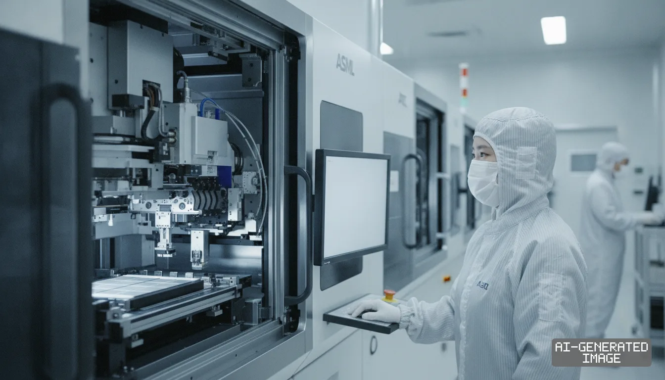
CXMT engineered its G5 architecture around deep ultraviolet immersion lithography tools rather than extreme ultraviolet systems. Washington and Dutch authorities strictly block shipments of EUV scanners to China.
The Hefei-based manufacturer applied self-aligned quadruple patterning — an iterative fabrication sequence of multi-step exposures and chemical etchings — to shrink the memory array active area half-pitch to 11.95 nanometers.
That dimension marks the physical distance between repeating conductive lines inside the memory array. The feature size places the platform on par with modern 10-nanometer-class architectures built by international competitors.
The company also integrated a high-k metal gate process to manage transistor leakage current, compressing the core cell functional area height to 6,762 nanometers.
Engineers achieved an array capacitor aspect ratio of 45:1 through modified structural flow and alternative chemical vapor deposition steps, the company said in a technical statement.
To accelerate design cycles without Western technical services, CXMT deployed a proprietary digital-twin modeling system across the product lifecycle, simulating process modifications before cutting physical wafers.
CXMT simultaneously announced mass production of two 24-gigabit low-power double data rate 5X memory components fabricated on the G5 line.
The memory chips feature 496-ball and 245-ball package configurations, offering 50% more storage capacity than the manufacturer's preceding mobile products.
The chips target premium mobile devices and portable electronics. Luo said the products have begun shipping to domestic smartphone manufacturers for integration into commercial flagship handsets.
The commercial rollout directly affects the dominant trio of global memory manufacturers: Samsung Electronics, SK hynix and Micron Technology. Together, the three incumbents control more than 90% of worldwide DRAM output.
Samsung Electronics and SK hynix hold heavy exposure to China's mobile hardware supply chain, selling billions of dollars of low-power DRAM annually to Chinese smartphone vendors.
CXMT generated approximately $8.6 billion in revenue in 2025, representing a 156% increase from the prior year as domestic procurement mandates steered device makers toward local suppliers.
The expansion of domestic DRAM supply eases pricing power for foreign incumbents in commodity and mobile sectors across China, allowing local device brands to substitute imported silicon.
Equipment manufacturers face a parallel shift in tool procurement patterns. Japanese supplier Tokyo Electron and domestic Chinese tool vendors have captured increased tooling demand as multi-patterning multiplies required deposition and etching cycles.
Quadruple patterning demands four times as many deposition and etch steps per layer compared with single-exposure EUV lithography, creating higher order volumes for non-controlled DUV processing equipment.
The company did not disclose its net commercial wafer yields, monthly wafer production volumes or unit manufacturing costs for the G5 platform.
CXMT also did not name the specific smartphone models or handset manufacturers receiving the new LPDDR5X chips.
While multiple patterning allows physical geometry scaling, industry engineers note that repeated processing steps inherently elevate defect density and wafer scrappage compared with single-exposure EUV lithography.
The United States Bureau of Industry and Security maintains scheduled interagency technical reviews in Washington to assess whether current parameter thresholds effectively limit foreign memory advancements.
Impact map
How this development propagates across the region and out to global buyers.
| Event | Korea | China | Japan | Global impact |
|---|---|---|---|---|
| CXMT G5 DRAM mass production | Samsung and SK hynix face Chinese mobile LPDDR5X share erosion | CXMT achieves 11.95nm half-pitch, raising gross die output by 50% | Tokyo Electron tool demand shifts as multi-patterning expands | US equipment sanctions challenged by DUV quadruple-patterning yields |
In this story
- Companies
- ChangXin Memory Technologies
- Exposed
- Samsung ElectronicsSK hynixMicron TechnologyTokyo Electron
- Policy
- Export Controls
- Impact
- Supply ChainCapexPricing
Track every Export Controls development →
Related briefings
- CXMT beats SK hynix and Micron in DRAM margin at 87.59% gross rate Also on ChangXin Memory Technologies, Micron Technology, SK hynix
- CXMT starts pilot HBM3E production as China accelerates AI chip self-reliance Also on ChangXin Memory Technologies, Micron Technology, SK hynix
- Naura and SMEE Accelerate Domestic Tool Shipments to Chinese Fabs Also on ChangXin Memory Technologies, Tokyo Electron, Export Controls
- China DRAM Makers Advance Proprietary Vertical Stacking to Counter HBM Export Curbs Also on ChangXin Memory Technologies, Export Controls
Sources
Reporting
Confidence: medium — how we grade this
The documents behind this briefing are linked above. East Asia Brief produces its English text with AI assistance under human editorial review, and does not translate or republish other outlets' articles. See our methodology and AI policy. Spotted an error? Tell us.
The Morning Brief
What changed in Korean, Chinese and Japanese industry overnight — and what it means for your supply chain. One email, weekday mornings, US time. Free.
The Morning Brief is in preparation. Leave your address and we will write to you once — when the first issue is ready. Nothing before that.