JSR opens South Korea EUV photoresist plant for 2nm chips
The 75 billion won facility in Ochang establishes local finishing lines for metal oxide resist, positioning the Japanese supplier adjacent to Samsung Electronics and SK hynix advanced fabs.
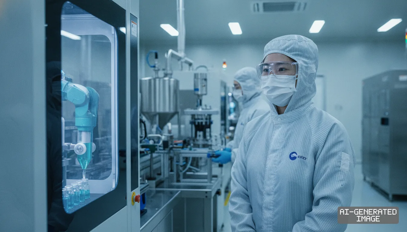
JSR Micro Korea completed a specialized semiconductor materials facility in Cheongju on Sept. 30, 2026, establishing domestic finishing lines for next-generation extreme ultraviolet photoresist.
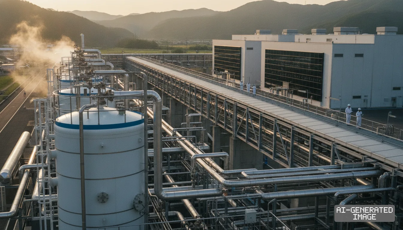
The plant operates inside the Ochang Foreign Investment Zone in North Chungcheong Province. It represents the first dedicated manufacturing site worldwide for the final production steps of metal oxide resist, the provincial government said.
The project represents an investment of 75 billion won ($56 million) and adds 26 manufacturing jobs. JSR commands approximately 30% of the global semiconductor photoresist market, according to ministry trade data.
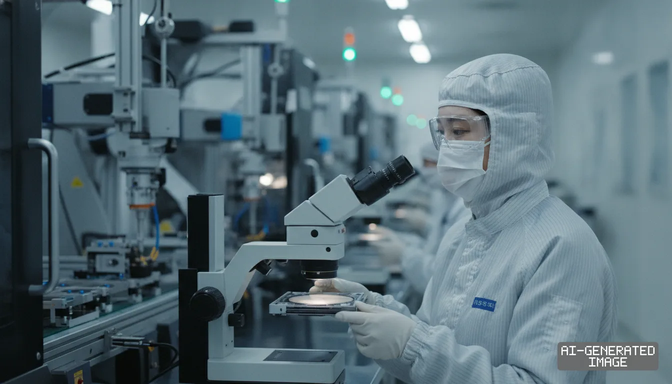
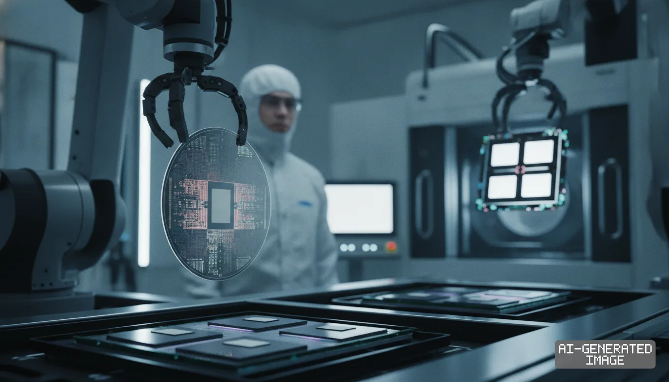
Metal oxide resist is an inorganic light-sensitive coating applied to silicon wafers during lithography. The metal compound absorbs extreme ultraviolet photons more effectively than organic formulations, preventing circuit lines from collapsing at sub-2nm dimensions.
Leading memory and foundry operators require the material to manufacture advanced logic chips and dense DRAM cells. Conventional chemically amplified resists suffer structural failures when chip geometries shrink past critical physical thresholds, process engineers said.
JSR commercialized the inorganic technology after acquiring Oregon-based materials developer Inpria Corp. in 2021. The Tokyo chemical group subsequently targeted localized fabrication to support South Korean contract foundries and memory fabricators directly.
The company signed an investment pact with North Chungcheong Province and Cheongju in August 2024. Municipal authorities granted zoning incentives to anchor cutting-edge lithography chemical production within the regional electronics cluster.
South Korea's Ministry of Trade, Industry and Energy attended the ground-breaking ceremony on Nov. 12, 2024. The ministry designated the facility a strategic asset for domestic semiconductor chemical supply chains, ministry records show.
The new lines position JSR adjacent to core manufacturing hubs operated by Samsung Electronics and SK hynix. Both chipmakers rely on extreme ultraviolet scanners to print high-density circuit layouts for artificial intelligence hardware.
Samsung Electronics uses extreme ultraviolet lithography across its Hwaseong and Pyeongtaek fabrication campuses. The contract manufacturer plans to deploy metal oxide resist for its sub-2nm gate-all-around process node, company technology roadmaps show.
SK hynix deploys extreme ultraviolet systems for 10nm-class DRAM production at its fabs in Icheon and Cheongju. Memory scaling requires precise chemical deposition to pattern billions of microscopic charge-storage capacitors without bridge defects, engineers said.
Domestic production reduces logistical risks for temperature-sensitive chemical formulations. Metal oxide resist requires stringent cold-chain transport to avoid chemical degradation during transit from overseas formulation plants, logistics handlers said.
The Ochang facility also protects South Korean chipmakers from regional trade and diplomatic friction. Tokyo instituted export curbs on photoresist shipments to South Korea in July 2019, disrupting bilateral component deliveries before bilateral settlements in 2023.
While those bilateral restrictions ended, chipmakers pressed essential suppliers to establish local backup operations. Building fabrication facilities inside South Korea guarantees uninterrupted chemical supply during international transport shocks or customs disputes, analysts said.
JSR established its first Korean manufacturing presence in Ochang in 2003, producing optical display materials. The new metal oxide facility broadens that Cheongju presence from flat-panel displays into advanced semiconductor lithography chemicals.
JSR President and Chief Executive Tetsuro Hori attended the completion ceremony on Wednesday alongside JSR Micro Korea President Takahiro Iijima. Provincial Governor Shin Yong-han and Cheongju Vice Mayor Shin Byeong-dae also took part.
Commercial operations at the Ochang plant are scheduled to begin during fiscal year 2026, ending March 31, 2027. JSR confirmed that schedule in its annual securities report filed to the Kanto Local Finance Bureau on June 24, 2026.
The annual report lists the Ochang facility under capital expenditure programs intended to expand electronic material manufacturing capacity. Management stated that initial product runs will undergo customer process validation prior to commercial volume scaling.
The provincial government notice does not state the plant's nameplate production capacity, and JSR has not published specific delivery dates for initial commercial shipments to Samsung Electronics or SK hynix.
As of Oct. 1, 2026, JSR Corporation has not published a formal completion announcement on its Tokyo corporate newsroom. The North Chungcheong Provincial Government statement remains the primary public confirmation of the plant's operational status.
State-backed investment fund Japan Investment Corp. completed a tender offer to acquire JSR in 2024. The privatization aimed to accelerate long-term capital investments and expand overseas manufacturing networks near major semiconductor fabrication hubs, filings show.
Initial test operations at the Ochang facility will continue through the fourth quarter of 2026. Domestic chip fabricators will examine sample chemical batches to certify etching selectivity and shelf life on silicon test wafers, provincial officials said.
Impact map
How this development propagates across the region and out to global buyers.
| Event | Korea | China | Japan | Global impact |
|---|---|---|---|---|
| JSR Ochang EUV MOR plant completion | Samsung and SK hynix gain local supply of sub-2nm MOR, cutting cold-chain import risks | no access to sub-2nm EUV lithography chemistry under multilateral export controls | JSR secures ~30% global resist share by locking in Korean foundry and DRAM accounts | Advanced packaging and sub-2nm AI chip manufacturing gains second-source resist capacity |
In this story
- Companies
- JSR CorporationJSR Micro Korea
- Tickers
- 005930.KS000660.KS
- Exposed
- Samsung ElectronicsSK hynix
- Policy
- Supply ChainSubsidies
- Impact
- Supply ChainCapexCompliance
Track every Supply Chain development → Track every Subsidies development →
Related briefings
- Japanese photoresist makers validate metal oxide resist lines for High-NA EUV chipmaking Also on JSR Corporation, Samsung Electronics
- Fujifilm plans $83 million chip materials plant in India Also on JSR Corporation
- Japan accelerates grants for rare-earth-reduced robot motor magnets under economic security act Also on Supply Chain, Compliance
- Japan bids to host permanent CPTPP secretariat to steer Asia-Pacific trade rules Also on Supply Chain, Compliance
Sources
Primary documents
Reporting
Confidence: high — how we grade this
The documents behind this briefing are linked above. East Asia Brief produces its English text with AI assistance under human editorial review, and does not translate or republish other outlets' articles. See our methodology and AI policy. Spotted an error? Tell us.
The Morning Brief
What changed in Korean, Chinese and Japanese industry overnight — and what it means for your supply chain. One email, weekday mornings, US time. Free.
The Morning Brief is in preparation. Leave your address and we will write to you once — when the first issue is ready. Nothing before that.