Fujifilm plans $83 million chip materials plant in India
The phased investment in Gujarat will supply chemical inputs to Tata Electronics' commercial wafer fab from fiscal 2028 under India's upgraded semiconductor incentive framework.
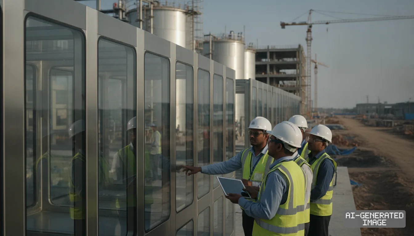
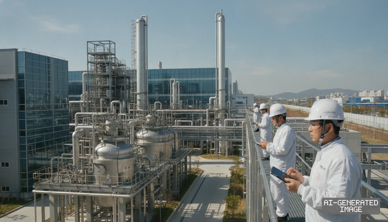
FUJIFILM Corporation said Sept. 17, 2026 it will invest 800 crore rupees ($83 million) to construct a semiconductor materials plant in Gujarat to supply Tata Electronics' new commercial fabrication facility.
The Tokyo-based company signed a memorandum of understanding with Tata Electronics during the Semicon India conference in New Delhi. The facility will occupy land in the Dholera Special Investment Region.
Tata Electronics is building an 91,000 crore rupee ($11 billion) front-end wafer fabrication plant at the Dholera site. That fab represents India's first commercial-scale silicon manufacturing project.
The foundry aims to process 300-millimeter silicon wafers across mature nodes ranging from 28 nanometers to 110 nanometers. Taiwan's Powerchip Semiconductor Manufacturing Corp. provides technology transfer for the facility.
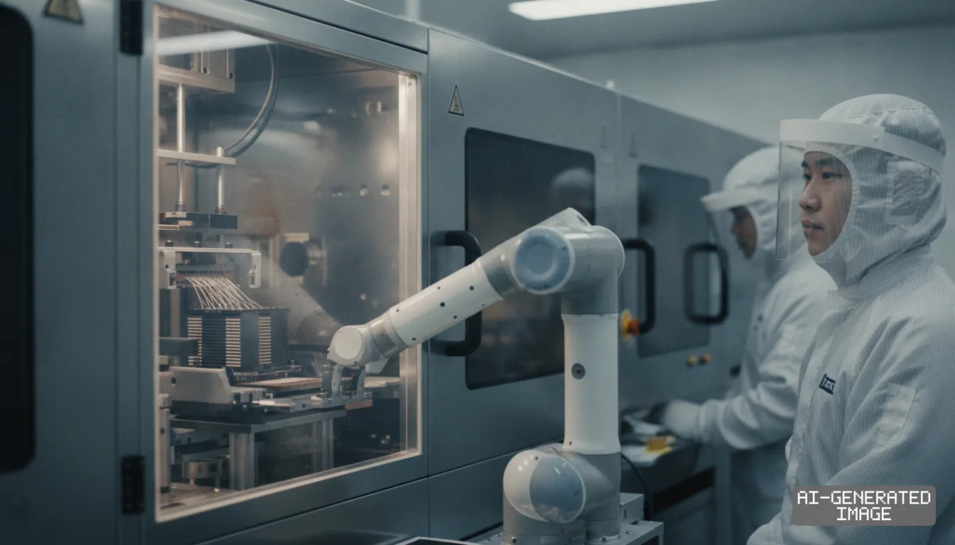
Construction of Fujifilm's chemical facility begins in October 2026. The initial phase will focus on manufacturing high-purity chemical formulations required for front-end wafer lithography and cleaning operations.
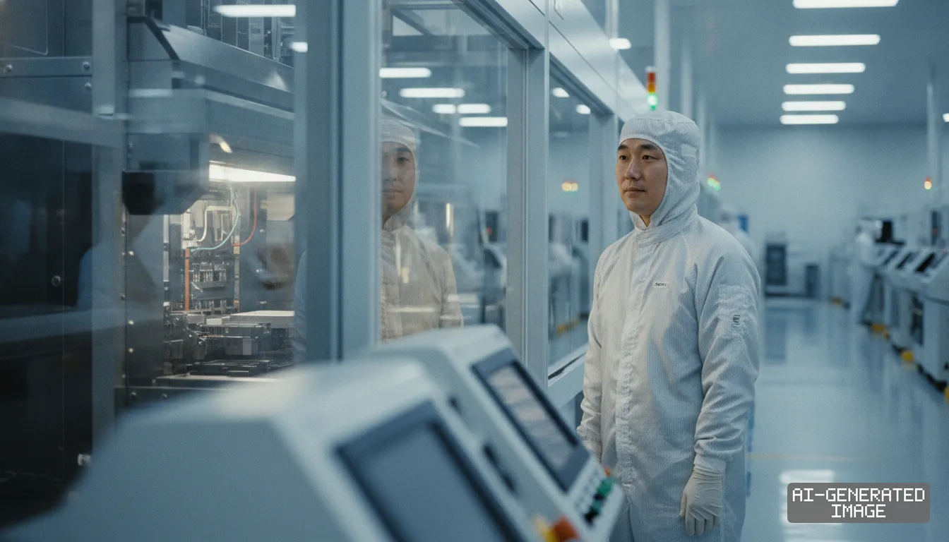
Commercial production from the first phase is scheduled to begin in fiscal year 2028. Output will move directly to cleanrooms at the neighboring Tata plant, the companies said.
A planned second phase will expand production into semiconductor surface-treatment agents and chemical mechanical planarization slurries. Slurries are abrasive chemical solutions used to polish wafer surfaces flat between circuit layers.
Fujifilm will also provide technical support and quality-assurance systems to domestic Indian chemical companies. That assistance is designed to qualify local suppliers for electronic-grade raw materials.
The project qualifies for financial incentives under the India Semiconductor Mission 2.0 framework approved by the Union Cabinet in July 2026. The upgraded policy subsidizes materials and equipment suppliers.
Tata Electronics is setting up a 363-acre vendor park in Dholera to house component and chemical providers. The chipmaker expects to host approximately 450 suppliers across that industrial cluster.
Chemical and gas suppliers must operate close to wafer fabs to prevent transport contamination and avoid supply disruptions. Liquid process chemicals degrade rapidly if stored or moved across long distances.
Japan's JSR Corporation also signed an agreement Sept. 17 to supply advanced photoresists and specialty chemicals to the Dholera fab. Tokyo Electron and other equipment makers are evaluating regional service centers.
Both companies conducted preliminary evaluations before executing the investment agreement. Fujifilm and Tata Electronics signed an initial cooperation pact in May 2025 and a preliminary memorandum with Gujarat officials in June 2026.
Tata Electronics is simultaneously developing an outsourced semiconductor assembly and test packaging site in Assam. That packaging facility will process finished wafers from the Dholera fab starting in 2027.
The joint release does not state whether Fujifilm will operate the Dholera plant as a wholly owned entity or through an equity joint venture with Tata Electronics.
The procurement schedule requires chemical qualification batches to undergo cleanroom testing six months before commercial wafer production starts. Gujarat authorities will hand over prepared industrial plots by late October 2026.
Specialty chemical manufacturers face strict purity standards when supplying front-end semiconductor fabrication lines. Impurities measured in parts per trillion can destroy microscopic circuit patterns on silicon wafers.
Locating chemical purification lines within the Dholera cluster reduces reliance on imported liquid containers from East Asian ports. Most semiconductor-grade solvents require temperature-controlled containers during marine transit.
Tata Electronics targets first commercial silicon shipments from the Dholera fab by mid-2027. The plant will produce microcontroller units, power management integrated circuits and display drivers for automotive and industrial buyers.
The Indian federal government covers up to 50% of capital expenditures for approved semiconductor fabrication projects. State governments provide additional fiscal incentives covering power infrastructure, water connections and land subsidies.
Japanese materials producers dominate global markets for photoresists, silicon wafers and CMP consumables. Establishing manufacturing footprints in India allows those suppliers to secure long-term purchase agreements before rival chemical firms arrive.
Tata Electronics signed 16 supplier agreements during the New Delhi conference, spanning materials, packaging tools and engineering services. European packaging supplier BESI and Dutch chipmaker Nexperia also committed to technical partnerships.
The joint project team will begin environmental permitting and architectural layout reviews for the Dholera parcel immediately following the October groundbreaking.
Impact map
How this development propagates across the region and out to global buyers.
| Event | Korea | China | Japan | Global impact |
|---|---|---|---|---|
| Fujifilm Dholera materials plant | no direct exposure, domestic chemical suppliers remain anchored to Korean memory fabs | no direct exposure, mature-node chemical supply remains focused on mainland foundries | Fujifilm and JSR secure early-mover supply positions at India's first commercial fab | semiconductor wet chemicals supply chain diversifies beyond East Asia toward South Asia |
In this story
- Companies
- FUJIFILM CorporationTata Electronics
- Tickers
- 4901.T
- Exposed
- Powerchip Semiconductor Manufacturing CorpJSR Corporation
- Policy
- SubsidiesEconomic Security
- Impact
- Supply ChainCapex
Track every Subsidies development → Track every Economic Security development →
Related briefings
- Japanese photoresist makers validate metal oxide resist lines for High-NA EUV chipmaking Also on JSR Corporation
- Japan Expands CMP Slurry Lines for Backside Power Also on FUJIFILM Corporation
- US and Japan weigh $19 billion GlobalFoundries fab under tariff pact
- Panasonic Energy opens Osaka battery hub for advanced cells
Sources
Reporting
Confidence: medium — how we grade this
The documents behind this briefing are linked above. East Asia Brief produces its English text with AI assistance under human editorial review, and does not translate or republish other outlets' articles. See our methodology and AI policy. Spotted an error? Tell us.
The Morning Brief
What changed in Korean, Chinese and Japanese industry overnight — and what it means for your supply chain. One email, weekday mornings, US time. Free.
The first issue goes out shortly. Sign up now and you will not miss it.