Intel tools Arizona Fab 62 to challenge TSMC on High-NA EUV
The chipmaker targets 2028 commercial output at its sixth Chandler facility, betting backside power delivery makes ASML scanners economic years before TSMC.
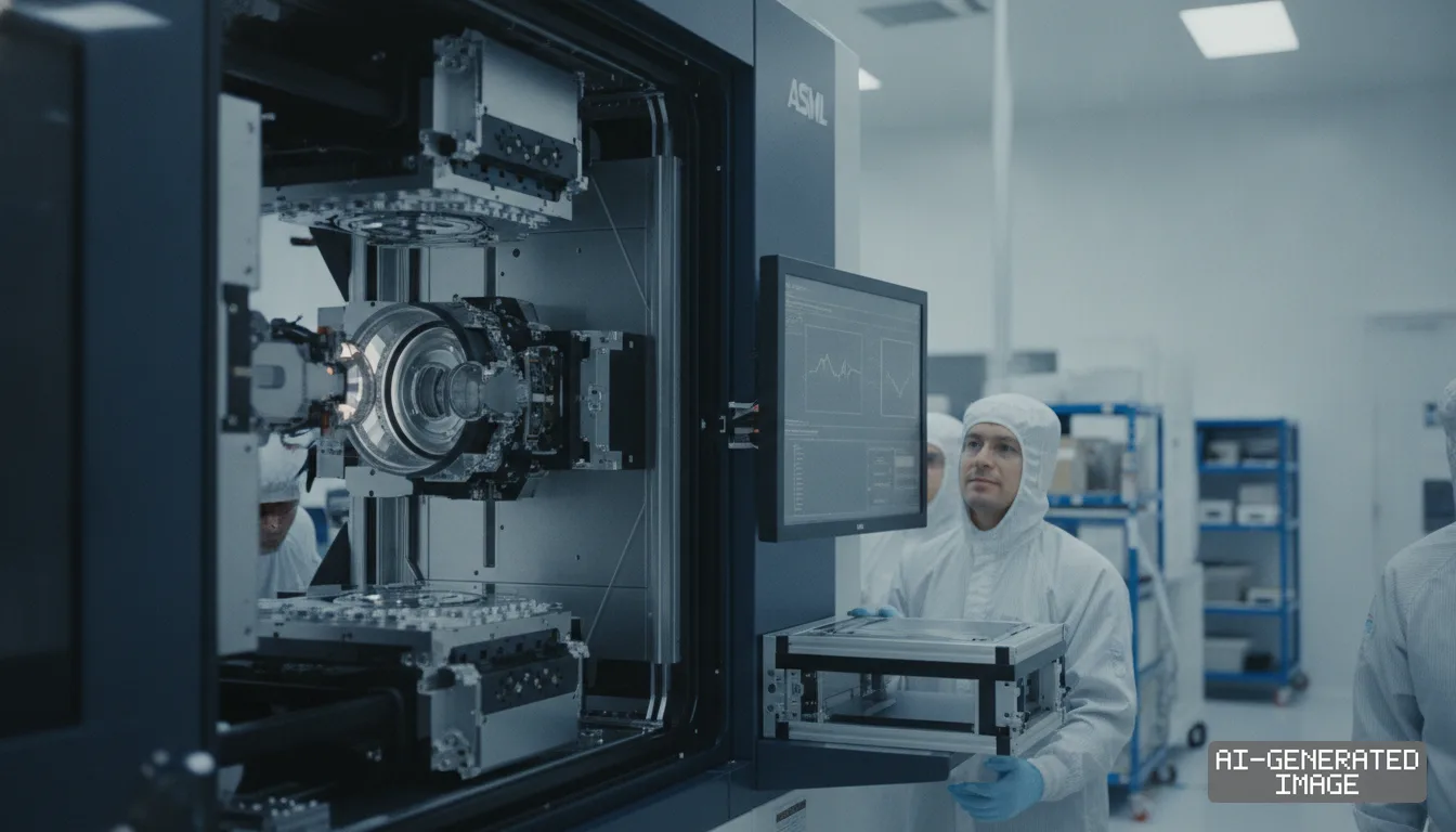
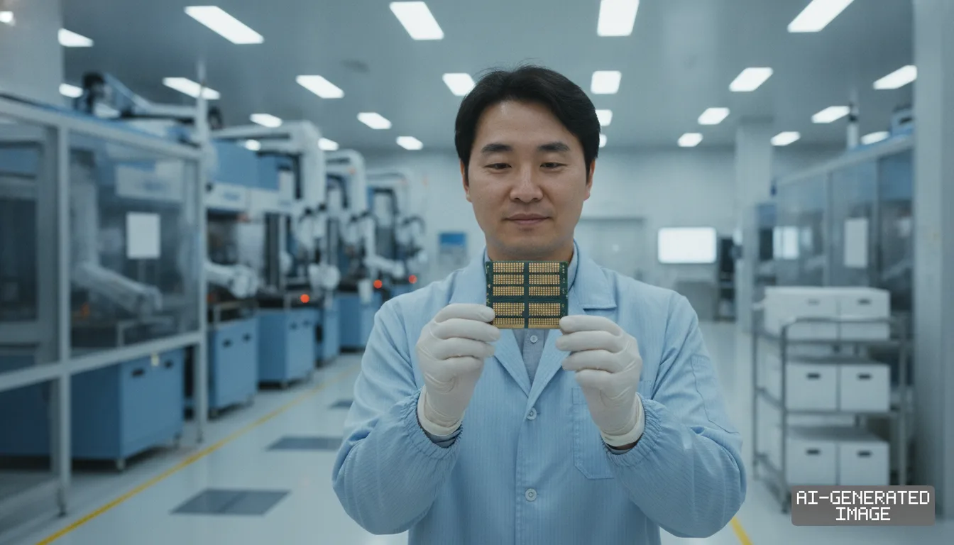
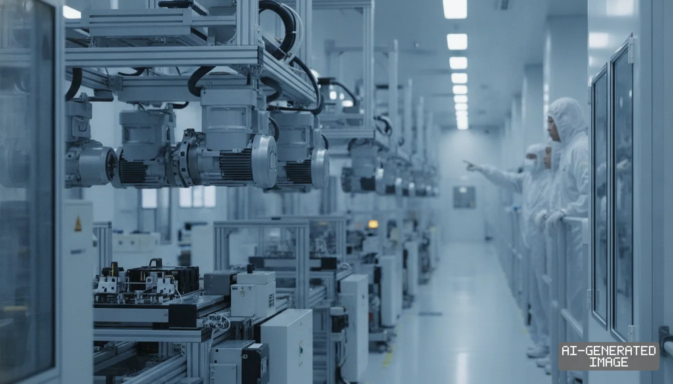
Intel Foundry started tool installation at its Fab 62 plant in Chandler, Arizona on Oct. 24, 2026, anchoring a high-numerical-aperture lithography strategy aimed at closing the scale gap with TSMC.
Each High-NA scanner from ASML Holding costs roughly $380 million, representing about 10% of total cleanroom tool outlays. Intel has processed more than one million test wafers on the systems.
The Arizona facility marks Intel's sixth high-volume manufacturing shell at Ocotillo. Production operations will begin by the end of 2028, said Naga Chandrasekaran, executive vice president and chief technology and operations officer.
Intel remains the only chipmaker running High-NA tools in high-volume production, Chandrasekaran said. The company integrated the 0.55 numerical aperture machines into its Oregon development lines during the summer of 2026.
TSMC, which commands roughly 62% of global contract foundry revenue, postponed commercial High-NA adoption until 2030. The Taiwanese chipmaker relies instead on 0.33 numerical aperture low-NA scanners using multiple patterning passes.
Intel intends to use early lithography access to regain manufacturing leadership after losing ground in advanced logic. The company plans to deploy the scanners commercially on its 14A node within three years.
Backside power delivery — which routes electricity through the rear of the wafer to clear surface area for transistors — makes the expensive tool economically viable, said Chris Auth, Intel vice president.
TSMC faces tighter frontside interconnect pitch constraints because it lacks backside routing on early 2-nanometer wafers, Auth said. Intel can print wider metal pitches in a single pass without multi-patterning defect risks.
Tool availability will determine the pace of foundry recovery rather than circuit physics, said Pushkar Ranade, Intel chief technology officer. Physical supply chains can double leading-edge wafer output rather than expand tenfold, Ranade said.
ASML produces fewer than 70 advanced lithography scanners each year across its Dutch factories. Tight delivery schedules across deposition, etching and inspection toolmakers restrict expansion rates across all chipmakers, Ranade said.
Intel designed its upcoming 14A process to reuse about 80% of the manufacturing machinery installed for 18A production. That tool reuse shields capital budgets as the company seeks volume orders from external customers.
Contract chip manufacturing operates with roughly 80% fixed overheads, meaning high cleanroom utilization governs financial returns. TSMC generates more than triple Intel's annual capital spending, establishing an operational barrier that lithography alone cannot quickly erode.
Samsung Electronics, the second-largest contract manufacturer with an 11% market share, delayed volume orders of ASML's 0.55 NA systems until 2027. Both Asian competitors view the optical split as premature for commercial yields.
High-NA lenses cut scanner exposure fields in half, forcing manufacturers to stitch masks together for large artificial intelligence accelerators. TSMC determined that stitch-line yield defects outweigh the speed gains of eliminating multi-patterning masks.
Intel sidestepped some masking penalties by dual-qualifying critical layers on its Panther Lake processor family in Oregon. That step lets engineers expose identical wafer layers on either older 0.33 NA or newer 0.55 NA scanners.
Matching defect densities on dual-qualified layers demonstrated that High-NA optics function reliably in production environments, Intel reported. However, early commercial wafers do not yet exploit the tighter circuit lines that 0.55 NA lenses deliver.
True geometric pitch scaling will only take effect once 14A reaches volume fabrication at Chandler and Oregon. That milestone requires external fabless design houses to complete full chip tape-outs on Intel's process design kits.
Intel 18A initially lacked complete electronic design automation toolkits, slowing third-party adoption, Auth said. The company is completing comprehensive design libraries for 14A to attract outside technology designers early in the cycle.
Commercial viability for Fab 62 depends on outside customer volume commitments for Intel 18A and 14A wafers. Hyperscale cloud providers have tested trial silicon but have delayed signing multi-year supply contracts.
In Ohio, construction workers mounted the first structural roof truss on the New Albany manufacturing facility. The Midwest site suffered recurring scheduling delays, pushing volume processor output back to at least 2030, Chandrasekaran said.
Federal subsidies under the US CHIPS Act supported construction of both Arizona Fab 62 and the Ohio complex. Washington disbursed $8.5 billion in direct grants to reinforce domestic manufacturing chains against East Asian concentration risks.
TSMC and Samsung also received US funding for plants in Arizona and Texas, intensifying regional competition for cleanroom technicians and support equipment. Both rivals have maintained their primary research and lithography tooling inside East Asia.
The company has not disclosed the initial monthly wafer starts allocated to Fab 62, and executives did not confirm the exact number of High-NA tools assigned to the site.
Tool qualification runs at Fab 62 will begin in late 2027, while TSMC reviews customer design kits for its A14 node in Hsinchu ahead of risk production in early 2028.
Impact map
How this development propagates across the region and out to global buyers.
| Event | Korea | China | Japan | Global impact |
|---|---|---|---|---|
| High-NA EUV commercial divergence | Samsung Electronics defers volume purchases to 2027, protecting 11% market share | Domestic fabs remain barred from EUV tools, relying on multi-patterned DUV lines | Equipment vendors redesign test inspection tools for 0.55 NA anamorphic optics | Intel deploys $380M scanners against TSMC's 62% foundry share ahead of 2028 output |
In this story
- Companies
- IntelTSMC
- Tickers
- INTC2330.TW
- Exposed
- ASMLSamsung Electronics
- Policy
- Subsidies
- Impact
- CapexSupply ChainPricing
Track every Subsidies development →
Related briefings
- Japan mask blank makers qualify High-NA EUV substrates for sub-2nm chips Also on ASML, Intel, TSMC
- TSMC widens High-NA EUV alliance to build 12-inch photomasks by 2031 Also on ASML, Intel, TSMC
- Taiwan clears TSMC fab site for sub-1.4nm chips at Longtan Also on ASML, Intel, TSMC
- Japanese photoresist makers validate metal oxide resist lines for High-NA EUV chipmaking Also on ASML, Intel, TSMC
Sources
Reporting
Confidence: medium — how we grade this
The documents behind this briefing are linked above. East Asia Brief produces its English text with AI assistance under human editorial review, and does not translate or republish other outlets' articles. See our methodology and AI policy. Spotted an error? Tell us.
The Morning Brief
What changed in Korean, Chinese and Japanese industry overnight — and what it means for your supply chain. One email, weekday mornings, US time. Free.
The Morning Brief is in preparation. Leave your address and we will write to you once — when the first issue is ready. Nothing before that.