Japan Expands CMP Slurry Lines for Backside Power
Japanese suppliers of chemical mechanical planarization consumables are accelerating capital spending across domestic manufacturing sites to support next-generation logic fabrication lines adopting backside power delivery networks. The transition to sub-2nm nodes including Taiwan Semiconductor Manufacturing Company's A16 platform and parallel angstrom-class architectures from Intel and Samsung Electronics relocates power distribution networks to the reverse side of the silicon wafer to eliminate interconnect bottlenecks. That architectural redesign separates direct-current power rails from frontside signal wiring, mitigating resistance-related voltage drops while requiring additional wafer thinning, carrier bonding, via-reveal, and metal planarization steps that increase consumable chemical mechanical planarization (CMP) polishing cycles per finished wafer.
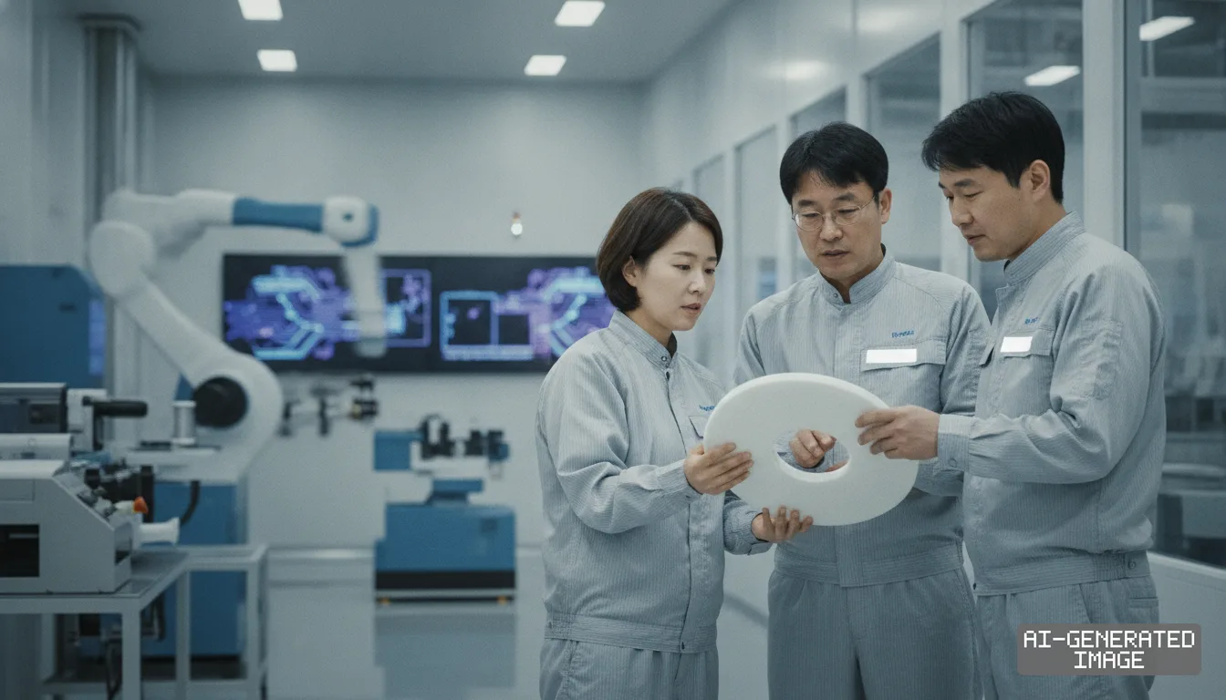
Consumable makers are positioning production lines to capture this structural increase in polishing demand. Fujibo Ehime Co., Ltd., the abrasive materials unit of Fujibo Holdings, has committed approximately 14 billion yen ($95 million) across two consecutive domestic capital expansion projects to scale its proprietary nonwoven-based CMP soft pad production capacity. On Nov. 28, 2025, Fujibo disclosed an 8.7 billion yen investment to erect a new manufacturing building and expand polishing pad lines at its Nyugawa Plant in Saijo, Ehime Prefecture, targeting commercial startup in the second half of fiscal year 2028. The company followed on Jan. 30, 2026, with an additional 5.3 billion yen allocation at its Oita Plant in Oita City to establish an integrated manufacturing and post-processing line for CMP soft pads, scheduled for operation in the second half of fiscal year 2028. The dual-site configuration increases aggregate pad output while establishing formal business continuity redundancy between Ehime and Oita.
FUJIFILM Corporation has expanded its domestic semiconductor materials footprint through FUJIFILM Electronic Materials Co., Ltd. to support both domestic fab projects and overseas foundry hubs. The company operates a CMP slurry production line at Kikuyo Town in Kumamoto Prefecture following an initial capital deployment of approximately 2 billion yen ($13 million), locating slurry synthesis adjacent to Japan Advanced Semiconductor Manufacturing (JASM). In parallel, Fujifilm completed a 20 billion yen advanced materials development and evaluation facility at its Shizuoka site, which supports specialized photoresists and planarization chemicals, and initiated construction of a dedicated facility at its Oita site to manufacture post-CMP cleaning formulations engineered to remove nano-particles, metal residues, and organic contaminants from finely pitched copper and dielectric surfaces.
Resonac Holdings has executed a 20 billion yen investment program across its domestic Yamazaki Works and Katsuta manufacturing site in Ibaraki Prefecture, alongside subsidiary operations in Taiwan and South Korea, raising group CMP slurry production and quality evaluation capacity by approximately 20 percent. The expansion centers on specialized abrasive formulations, including nano-ceria and high-purity colloidal silica slurries designed for tight-pitch logic and three-dimensional memory devices. Ceria-based slurries achieve high polishing selectivity between silicon oxide and silicon nitride barriers, suppressing dishing and micro-scratch defects during critical shallow trench isolation and interlayer dielectric planarization passes.
While corporate disclosures cite broad demand drivers including generative artificial intelligence hardware, multi-layer memory scaling, and transistor miniaturization the emergence of backside power delivery represents a specific volume multiplier for planarization tooling and consumables. In conventional frontside manufacturing, power lines share routing tracks with clock and data signal lines in the upper metallization stack. Under backside power rail architectures, the frontside logic transistors and signal interconnect layers are fabricated first, bonded face-down to a temporary carrier wafer, and mechanically ground and polished from the backside until the active silicon substrate is thinned to less than one micrometer.
The subsequent via-reveal and backside metallization stages require multiple selective CMP passes to uncover nanoscale power contacts without eroding adjacent silicon. Planarization engineers must alternate between silicon oxide slurries, metal-selective copper slurries, and barrier-removal slurries across both sides of the bonded substrate. Uneven pad wear, particle agglomeration, or inconsistent slurry selectivity can induce wafer bow, unbonded edge delamination, or contact resistance spikes across the exposed backside vias.
These mechanical requirements lengthen qualification timelines for consumable suppliers. Leading foundries evaluate pad elasticity, groove patterns, slurry particle size distributions, and chemical corrosion inhibitors over multiple quarters of test wafer runs before freezing bill-of-materials specifications for high-volume nodes. Once a specific pad-and-slurry formulation clears process qualification for a node's baseline yield recipe, switching vendors introduces defectivity risks that foundries avoid during commercial volume ramps.
Japanese materials producers currently maintain a strong aggregate footprint in global CMP consumables, competing against United States suppliers including Entegris, DuPont, and Cabot Microelectronics across specific chemical formulations and pad segments. By building dedicated synthesis capacity, local evaluation laboratories, and multi-site production networks within Japan, suppliers aim to lock in formula certifications with domestic ventures such as Rapidus in Hokkaido and major Asian foundry clients across Taiwan and South Korea.
Fujibo's Nyugawa and Oita pad lines remain scheduled to enter mass production in the second half of fiscal year 2028, coinciding with foundry timelines for commercial angstrom-class logic output. Resonac and Fujifilm continue commercial shipments of ceria and copper CMP consumables from their expanded facilities in Ibaraki, Kumamoto, and Shizuoka while qualifying specialized chemical cleaning and planarization formulations for customer-specific sub-2nm node integrations.
Impact map
How this development propagates across the region and out to global buyers.
| Event | Korea | China | Japan | Global impact |
|---|---|---|---|---|
| BSPDN node transition | foundry qualification | advanced node barrier | pad and slurry capex | wafer planarization cost |
In this story
- Companies
- Fujibo HoldingsFUJIFILM CorporationResonac Holdings
- Tickers
- 3104.T4901.T4004.T
- Exposed
- Taiwan Semiconductor Manufacturing CompanyIntelSamsung ElectronicsRapidus
- Policy
- Economic SecuritySubsidies
- Impact
- Supply ChainCapexOrder Book
Track every Economic Security development → Track every Subsidies development →
Related briefings
- Fujifilm plans $83 million chip materials plant in India Also on FUJIFILM Corporation
- Rapidus begins trial runs on 2nm pilot line in Hokkaido ahead of 2027 target Also on Resonac Holdings, Rapidus, Order Book
- Sojitz and NRS agree to build Tata fab chemical supply chain in India Also on FUJIFILM Corporation
- East Asia accelerates 8-inch silicon carbide capacity race as power chip makers scale output Also on Resonac Holdings
Sources
Reporting
- fujibo.co.jp
- fujifilm.com
- communicationstoday.co.in
- pressreleasepoint.com
- transparencymarketresearch.com
Confidence: medium — how we grade this
The documents behind this briefing are linked above. East Asia Brief produces its English text with AI assistance under human editorial review, and does not translate or republish other outlets' articles. See our methodology and AI policy. Spotted an error? Tell us.
The Morning Brief
What changed in Korean, Chinese and Japanese industry overnight — and what it means for your supply chain. One email, weekday mornings, US time. Free.
The Morning Brief is in preparation. Leave your address and we will write to you once — when the first issue is ready. Nothing before that.