ASML expands Japan workforce to 700 to support Rapidus 2nm and TSMC fabs
The Dutch lithography supplier plans a 40% headcount increase by 2030 to install and maintain EUV equipment for cutting-edge foundry projects.
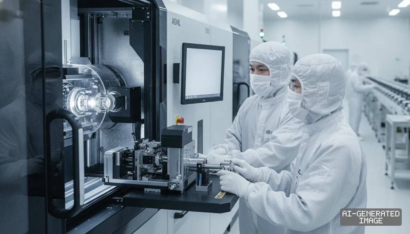
ASML said Sept. 3 it will expand its Japanese workforce to 700 employees by 2030, bolstering field engineering support for domestic foundry venture Rapidus and Taiwan Semiconductor Manufacturing Co.
Shojiro Fujiwara, president of ASML Japan, announced the expansion during a press conference. The target represents a 40% increase from the Dutch equipment maker's current payroll of 500 workers in Japan.
The revised hiring target supersedes an earlier roadmap released in September 2023. At that time, ASML planned to raise Japanese headcount from 400 to roughly 560 employees by 2028.
The decision underscores growing operational demands as Japan attempts to re-establish domestic production of advanced logic semiconductors after decades of relying on overseas foundries for sub-10-nanometer parts.
Rapidus forms the primary catalyst for the technical support ramp. The state-backed venture aims to begin mass production of 2-nanometer logic chips during fiscal 2027 at its IIM-1 facility in Chitose, Hokkaido.
Lithography systems represent the critical bottleneck in that timeline. In December 2024, Rapidus took delivery of Japan's first commercial extreme ultraviolet system, an ASML NXE:3800E scanner installed at the Chitose plant.
The NXE:3800E delivers higher wafer throughput than prior scanner generations, processing more than 200 wafers per hour. Operating the hardware requires round-the-clock maintenance to prevent costly tool downtime.
Extreme ultraviolet machines use 13.5-nanometer wavelength light to print circuit features onto silicon wafers. Each system requires specialized on-site engineers to manage mirror optics, vacuum chambers and tin-droplet laser sources.
ASML opened a technical support center in Hokkaido to service the Chitose facility. Field engineers at the base provide continuous system maintenance, component replacements and optical calibration for pilot-line testing.
Rapidus began trial wafer processing on its Chitose pilot line in April 2025. The company verified initial test wafers using gate-all-around transistor architecture, the structural design required for 2-nanometer logic fabrication, in July 2025.
The Japanese foundry is also preparing for subsequent technology nodes. Rapidus plans to build a second fab in Chitose to support 1.4-nanometer chip production targeted for 2029, which will require further lithography capacity.
Commercial viability hinges on pricing and manufacturing yields. Rapidus President Atsuyoshi Koike said in July 2026 that the firm aims to price 2-nanometer wafers between 3 million and 3.5 million yen ($18,500 to $21,500).
Customer engagement has expanded alongside factory preparations. Rapidus has initiated technical discussions with more than 60 semiconductor design firms, seeking commitments ahead of its planned 2027 volume production schedule.
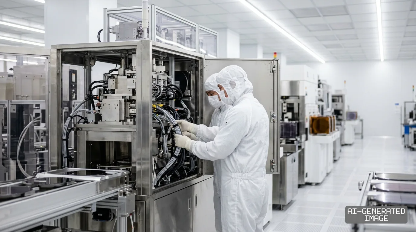
An unserviced lithography scanner can halt an entire cleanroom line. Having dedicated vendor technicians on site reduces tool recovery times and helps foundry engineers stabilize production yields.
ASML engineers will also support Taiwan Semiconductor Manufacturing Co. in Kumamoto Prefecture. TSMC operates manufacturing facilities there through its majority-owned subsidiary, Japan Advanced Semiconductor Manufacturing, commonly known as JASM.
The Taiwanese foundry opened its first Kumamoto fab in early 2024 to produce mature logic nodes. It is preparing subsequent capacity additions that introduce more advanced manufacturing processes to the Kyushu production base.
JASM counts Sony Semiconductor Solutions and automotive supplier Denso as minority shareholders. The joint venture anchors automotive microcontroller and image sensor packaging inside southern Japan.
ASML previously enlarged its Kumamoto technical base to 40 field engineers in 2024. The latest workforce plan ensures sustained support as tool counts rise across both regional production hubs.
Japan's Ministry of Economy, Trade and Industry, which orchestrates the national chip revitalization program, has committed trillions of yen to subsidize wafer fabs and equipment installations across Hokkaido and Kyushu.
The ministry completed an additional capital injection of approximately $1 billion into Rapidus in June 2026. The funds support fab infrastructure, equipment purchases and research on subsequent 1.4-nanometer process technology.
State funding covers a significant share of initial capital spending. Government officials view leading-edge logic fabrication as an essential security asset to protect supply chains against potential regional conflicts.
Other global toolmakers have mirrored the staffing push. Applied Materials and Lam Research expanded their Japanese field engineering teams to service cleanrooms across Hokkaido and Kumamoto.
Fujiwara said Japan's semiconductor industry will continue expanding amid shifting regional supply chains. Geopolitical tensions have led chipmakers and governments to build redundant manufacturing capacity outside Taiwan and South Korea.
The company has not disclosed the exact headcount division between its Hokkaido and Kumamoto operations. ASML also withheld the capital expenditure figure allocated for the Japan expansion.
Securing specialized engineers remains an operational hurdle across East Asia. Precision lithography servicing requires extensive technical training, and rival toolmakers are competing for the same pool of Japanese hardware specialists.
To address staffing constraints, ASML has partnered with Japanese universities and technical institutes. The initiative aims to train domestic engineering graduates on cleanroom protocols and EUV optical maintenance procedures.
Tool deliveries to Japanese fabs will accelerate as Rapidus transitions from trial testing to pre-production runs. Additional scanners require dedicated support personnel to complete cleanroom hookups and optical alignment.
Rapidus is scheduled to continue pilot-line validation at Chitose through 2026, while ASML phases in local engineering hires to meet its 2030 domestic workforce target.
Impact map
How this development propagates across the region and out to global buyers.
| Event | Korea | China | Japan | Global impact |
|---|---|---|---|---|
| ASML Japan workforce expansion | — | — | engineering support for Rapidus and TSMC | advanced packaging and 2nm node readiness |
In this story
- Companies
- ASMLRapidusTaiwan Semiconductor Manufacturing Co.
- Tickers
- ASML2330.TW
- Exposed
- Sony GroupDensoApplied MaterialsLam Research
- Policy
- SubsidiesEconomic Security
- Impact
- Supply ChainCapexCost Structure
Track every Subsidies development → Track every Economic Security development →
Related briefings
- Air Liquide invests €170M to expand Japan chip gas capacity Also on Denso, Sony Group, Rapidus
- Japan seeks $2.6B for Rapidus after pledging $21B to US fabs Also on Sony Group, Rapidus, Cost Structure
- Rapidus forms 17-firm design alliance to back 2nm chip ramp Also on Sony Group, Rapidus, Subsidies
- Japan Prefectures Woo Taiwan Chip Vendors With Site Grants Also on Sony Group, Taiwan Semiconductor Manufacturing Co., Cost Structure
Sources
Reporting
Confidence: medium — how we grade this
The documents behind this briefing are linked above. East Asia Brief produces its English text with AI assistance under human editorial review, and does not translate or republish other outlets' articles. See our methodology and AI policy. Spotted an error? Tell us.
The Morning Brief
What changed in Korean, Chinese and Japanese industry overnight — and what it means for your supply chain. One email, weekday mornings, US time. Free.
The Morning Brief is in preparation. Leave your address and we will write to you once — when the first issue is ready. Nothing before that.