TSMC and Samsung set High-NA EUV roadmaps for sub-2nm nodes
The foundries committed to ASML's next-generation lithography tools to bridge patterning limits, facing machine costs near $400 million per unit.
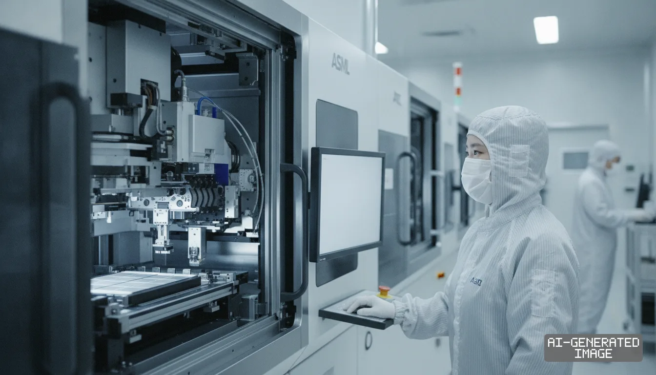
TSMC and Samsung Electronics formalized deployment roadmaps for ASML Holding NV's High-NA EUV lithography systems on Sept. 19, locking in commercial adoption schedules for sub-2-nanometer fabrication.
The decision commits both foundries to ASML's twin-stage EXE platform, where each tool costs an estimated $400 million. That single scanner represents nearly 30% of total equipment expense for a modern 300-millimeter cleanroom module.
High-NA EUV systems raise numerical aperture — the light-gathering capacity of the projection optics — from 0.33 to 0.55. This optical improvement shrinks printed feature dimensions by a factor of 1.7, letting fabs print microscopic lines with 40% higher image contrast.
Without High-NA tools, foundries must print sub-2-nanometer features using multi-patterning on standard EUV equipment. That process requires multiple exposure passes per layer, compounding mask alignment errors and lowering finished wafer yields.
The soaring cost of lithography hardware forces chipmakers to reassess node economics. Outfitting an advanced manufacturing facility with two dozen High-NA scanners now demands capital investments exceeding $20 billion, concentrating capital risk among fewer market participants.
Because ASML holds an effective monopoly on extreme ultraviolet equipment, foundries have no alternative commercial machinery vendor. Asian chipmakers must align with the Dutch manufacturer's delivery schedules and pricing terms to execute their advanced technology roadmaps.
TSMC scheduled high-volume manufacturing with High-NA EUV to begin in 2030. The Taiwanese foundry plans to run initial production for its 2-nanometer N2 node and subsequent A16 process on existing low-NA tools using multi-patterning.
Company leadership elected to delay High-NA insertion until late-stage A14 production. Postponing deployment spares TSMC immediate equipment depreciation charges while allowing industry peers to absorb early process integration costs and line downtime.
To overcome optical field limits, TSMC and ASML formed an initiative to transition the sector to 12-inch photomasks. The partners scheduled a pilot mask line for 2031, targeting full production readiness by 2033.
Standard High-NA optics halve the scanner exposure field, forcing foundries that rely on six-inch masks to stitch two exposures together. The 12-inch photomask format eliminates stitching seams, protecting scanner throughput on large artificial intelligence processors.
Samsung Electronics announced plans to deploy High-NA EUV on advanced dynamic random-access memory lines by 2028. The South Korean manufacturer aims to secure the memory sector's first commercial rollout of 0.55 NA scanners.
For its logic foundry operations, Samsung plans to evaluate High-NA EUV deployment for its 1.4-nanometer SF1.4 process around 2029. Samsung also joined the ASML-led large mask consortium to co-develop 12-inch photomask infrastructure.
Samsung treats early High-NA adoption in memory as essential for next-generation high-bandwidth memory production. Tighter DRAM circuit patterning yields smaller die footprints, permitting denser vertical stacking in artificial intelligence memory stacks.
Intel Foundry operates early High-NA test tools at its Hillsboro site in Oregon. Intel processed more than one million test wafers across development lines, creating competitive pressure that forced Asian rivals to publish formal integration schedules.
The industry shift toward 12-inch photomasks requires complete tooling re-engineering across the semiconductor supply chain. Mask blank fabricators, inspection scanner builders, chemical cleaning units and transport pods must all accommodate the wider substrate format.
Japanese suppliers including Lasertec and Shin-Etsu Chemical must develop 12-inch blank materials and actinic inspection platforms. None of these ancillary systems exist in commercial volume today, requiring multi-year development lead times before 2031.
For fabless chip customers, high scanner capital costs will raise contract wafer prices. Early 2-nanometer wafers already trade above $30,000 each, and sub-2-nanometer wafers could top $40,000 under High-NA depreciation schedules.
The official announcements do not state contract pricing for the scanners, and neither manufacturer has disclosed the exact quantity of commercial tools secured under initial purchase agreements.
If wafer processing costs outpace architectural performance gains, semiconductor design firms may delay migrating from mature 3-nanometer nodes. Elevated equipment amortization risks compressing foundry margins during the multi-year transition toward 12-inch mask standards.
The Large Size Mask Consortium convenes technical working groups ahead of the 2031 pilot deadline, while Samsung begins cleanroom readiness preparations at its Pyeongtaek campus for initial system deliveries.
Impact map
How this development propagates across the region and out to global buyers.
| Event | Korea | China | Japan | Global impact |
|---|---|---|---|---|
| High-NA EUV roadmap adoption | Samsung targets 2028 DRAM rollout and SF1.4 logic development | Domestic fabs face widening technology gap, cut off from advanced EUV tools | Tool and blank makers face re-engineering costs for 12-inch mask formats | Chipmakers absorb $400 million tool costs, pushing sub-2nm wafer prices over $40,000 |
In this story
- Companies
- TSMCSamsung ElectronicsASML Holding
- Tickers
- 2330.TW005930.KSASML.AS
- Exposed
- IntelLasertecShin-Etsu Chemical
- Policy
- Economic Security
- Impact
- CapexSupply ChainPricing
Track every Economic Security development →
Related briefings
- TSMC revenue rises 53% on AI demand to record NT$514 billion Also on ASML Holding, Intel, Samsung Electronics
- TSMC warns AI cannot solve physical barriers for 1.4nm chips Also on ASML Holding, Intel, Samsung Electronics
- Naura and SMEE Accelerate Domestic Tool Shipments to Chinese Fabs Also on ASML Holding
- TSMC widens High-NA EUV alliance to build 12-inch photomasks by 2031 Also on TSMC, Intel, Samsung Electronics
Sources
Reporting
Confidence: medium — how we grade this
The documents behind this briefing are linked above. East Asia Brief produces its English text with AI assistance under human editorial review, and does not translate or republish other outlets' articles. See our methodology and AI policy. Spotted an error? Tell us.
The Morning Brief
What changed in Korean, Chinese and Japanese industry overnight — and what it means for your supply chain. One email, weekday mornings, US time. Free.
The Morning Brief is in preparation. Leave your address and we will write to you once — when the first issue is ready. Nothing before that.