TSMC adds five packaging fabs in Chiayi to ease AI crunch
Taiwan's consultation for a 198.65-hectare Chiayi Science Park expansion clears the path for TSMC to construct five more advanced packaging lines, bringing its regional footprint to 10 facilities.
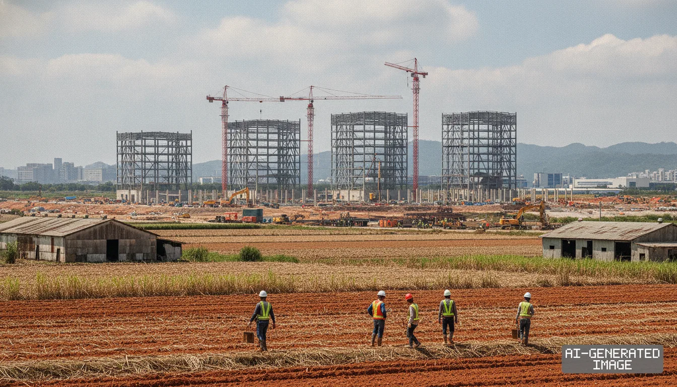
Taiwan Semiconductor Manufacturing Co. advanced plans Sept. 28 to construct five additional advanced packaging fabs in southern Taiwan, responding to persistent capacity shortages for artificial intelligence processor integration.
The prospective facilities will occupy a 198.65-hectare expansion zone at Chiayi Science Park in Taibao City. The land consists of agricultural plots leased from state-owned enterprise Taiwan Sugar Corp.
Constructing five more plants will increase TSMC’s total footprint in Chiayi to 10 advanced packaging facilities. The scale makes the site the world’s largest back-end cluster for high-density chip assembly.
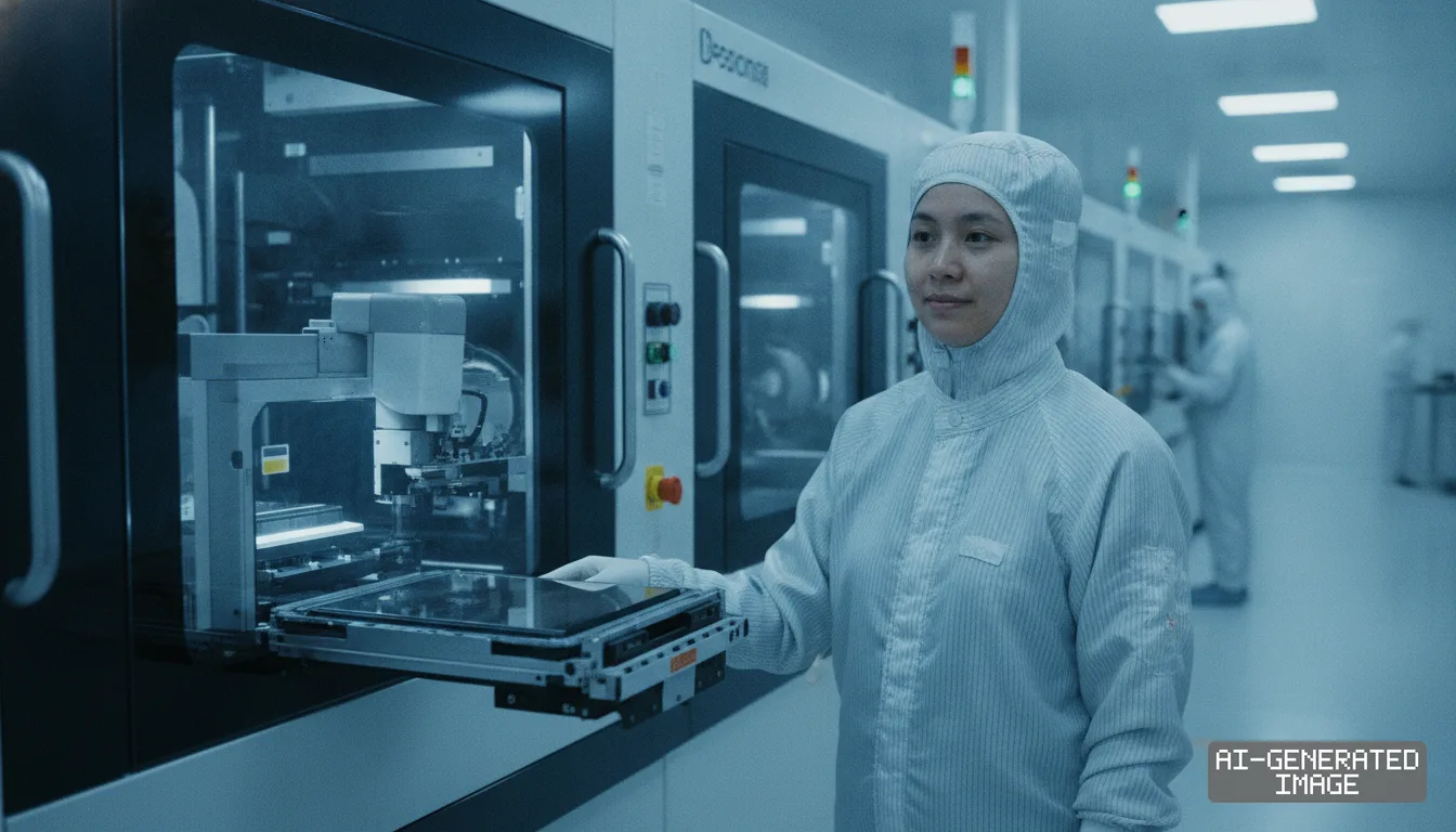
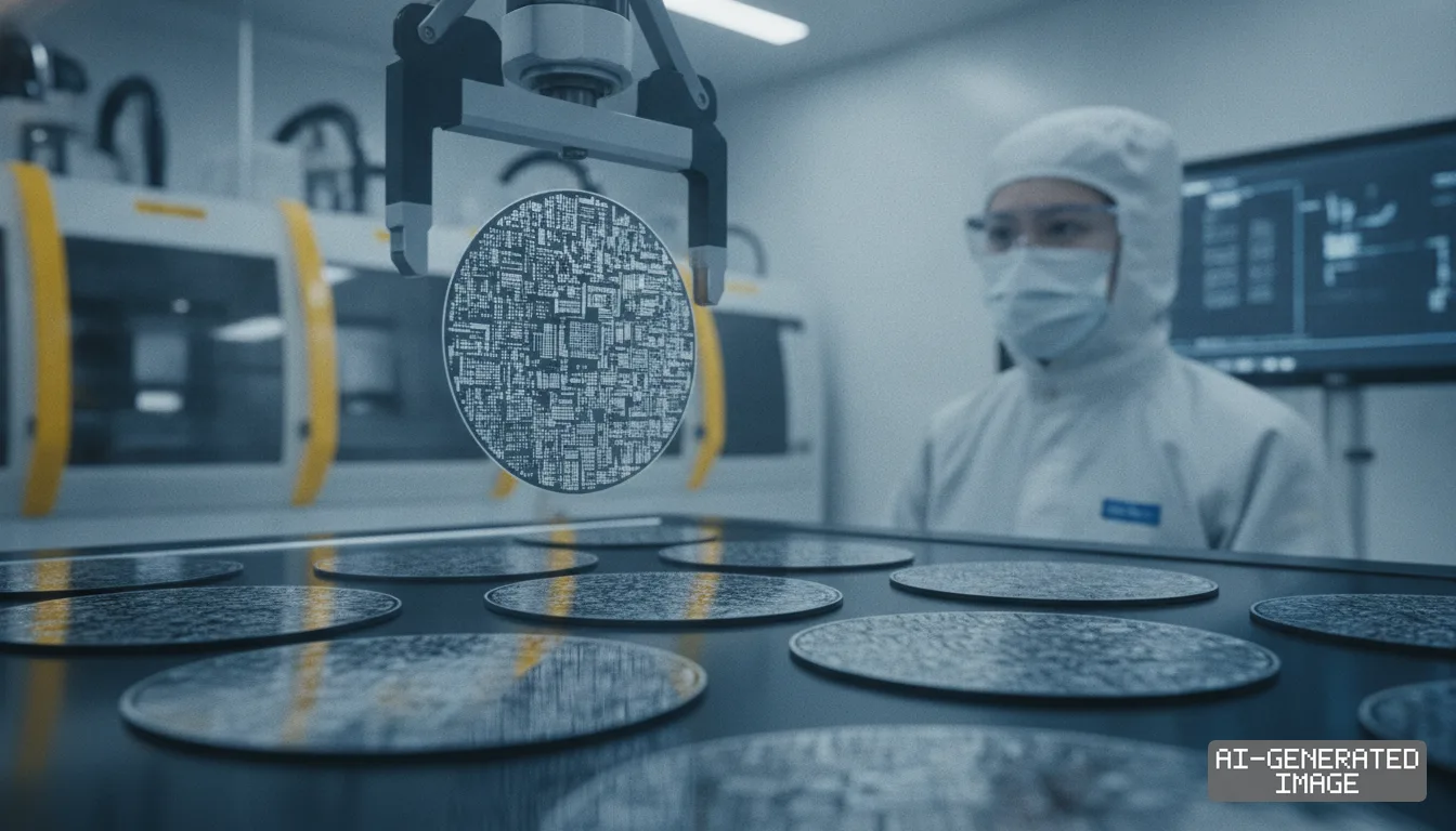
The expansion targets Chip-on-Wafer-on-Substrate packaging, known as CoWoS. The proprietary process places logic dies and high-bandwidth memory side by side on a silicon interposer, forming the primary physical bottleneck in AI hardware shipments.
TSMC operates under an existing phased development schedule at the Chiayi complex. The company is completing equipment move-in for Phase 1 fabs P1 and P2, with commercial mass production scheduled for 2027.
Phase 2 encompasses fabs P3, P4 and P5 on a 90-hectare plot approved earlier this year. Foundation work on fab P3 began in mid-2026, with full construction across all three units targeted for completion by 2031.
The newly reported five packaging fabs represent Phase 3 of the science park roadmap. The project emerged after Taiwan’s central authorities moved to accelerate regional industrial land allocations for high-performance computing supply chains.
Physical constraints in advanced wafer fabrication have pushed performance gains into back-end integration. As conventional transistor scaling yields diminish, compute throughput depends on interconnect speed and proximity between processing dies and memory stacks.
Customer demand for CoWoS packaging continues to exceed available manufacturing capacity. Nvidia absorbs more than 50% of TSMC’s current packaging allocation, leaving graphics processing unit lead times tied directly to back-end throughput.
Advanced Micro Devices and Apple also retain dedicated production allocations on the same assembly lines. Hyperscale cloud providers developing bespoke inference silicon add further demand pressure on TSMC’s southern packaging lines.
TSMC projects its total CoWoS production capacity will expand at a compound annual rate exceeding 80% through 2027. The company is adding cleanroom space across both central and southern Taiwan to handle commitments.
The foundry operates 19 advanced wafer fabs and packaging facilities across Taiwan, according to the Ministry of Economic Affairs. TSMC has 13 additional facilities under construction in Hsinchu, Taichung, Chiayi, Tainan and Kaohsiung.
The Chiayi buildout forms part of a broader government program connecting southern industrial hubs. The National Science and Technology Council is linking Chiayi with sites in Tainan, Kaohsiung and Pingtung to build an integrated technology corridor.
The massive capital deployment is accelerating a structural shift between wafer foundries and outsourced semiconductor assembly and test providers. Foundries are absorbing high-margin packaging steps that once belonged exclusively to dedicated assembly contractors.
ASE Technology Holding accounts for roughly 25% of global outsourced packaging revenue. While ASE dominates traditional chip packaging, contract foundries retain exclusive control over front-line 2.5D packaging workflows required for cutting-edge accelerators.
Traditional packaging providers maintain volume assembly contracts for automotive, communications and consumer silicon. Major accelerator vendors bypass independent packaging subcontractors entirely, purchasing bundled wafer fabrication and interposer bonding directly from TSMC.
Advanced 2.5D packaging lines require sub-micron alignment tools and high-grade cleanrooms comparable to front-end wafer fabs. Those facility requirements create capital barriers that independent assembly contractors struggle to match without direct customer subsidies.
Taiwanese authorities project the fully operational Chiayi Science Park will generate more than 300 billion New Taiwan dollars ($9.35 billion) in annual industrial output. The industrial complex will support approximately 9,000 local technical jobs.
Taiwan’s National Science and Technology Council officially initiated the regulatory process for the expansion on Sept. 24. The agency published a public consultation notice designating the 198.65-hectare project as the Chiayi Park Phase 2 scale-up.
The mandatory 30-day public comment window closes Oct. 24, 2026. Following that consultation period, the science park administration will submit a formal feasibility study to the Executive Yuan for central government review.
The expansion must subsequently secure formal approvals through statutory Environmental Impact Assessments and regional zoning modifications. Planners must verify regional water delivery schedules and electrical transmission capacity before awarding construction tenders.
TSMC has not filed a material disclosure on the Taiwan Stock Exchange or issued a corporate statement confirming capital expenditures, construction schedules or equipment procurement for the prospective Phase 3 packaging facilities.
Impact map
How this development propagates across the region and out to global buyers.
| Event | Korea | China | Japan | Global impact |
|---|---|---|---|---|
| Chiayi packaging fab expansion | SK hynix safeguards HBM4 integration slots alongside foundry wafer runs | CXMT remains excluded from advanced CoWoS packaging ecosystem | Tokyo Electron books additional coater-developer and etching tool shipments | Server makers ease delivery lead times as CoWoS throughput expands |
In this story
- Companies
- TSMC
- Tickers
- 2330.TW
- Exposed
- ASE Technology HoldingNvidia
- Policy
- Economic SecuritySubsidies
- Impact
- CapexSupply ChainPricing
Track every Economic Security development → Track every Subsidies development →
Related briefings
- Taiwan breaks ground on TSMC packaging base to relieve CoWoS limits Also on ASE Technology Holding, Nvidia
- Silicon interposer scaling drives foundry and OSAT shifts in 3.5D chiplets Also on ASE Technology Holding
- JCET expands automotive radar SiP packaging lines to capture ADAS sensor demand Also on ASE Technology Holding
- SK hynix starts $4 billion packaging plant in Indiana to feed US AI Also on TSMC, Nvidia
Sources
Reporting
Confidence: medium — how we grade this
The documents behind this briefing are linked above. East Asia Brief produces its English text with AI assistance under human editorial review, and does not translate or republish other outlets' articles. See our methodology and AI policy. Spotted an error? Tell us.
The Morning Brief
What changed in Korean, Chinese and Japanese industry overnight — and what it means for your supply chain. One email, weekday mornings, US time. Free.
The Morning Brief is in preparation. Leave your address and we will write to you once — when the first issue is ready. Nothing before that.