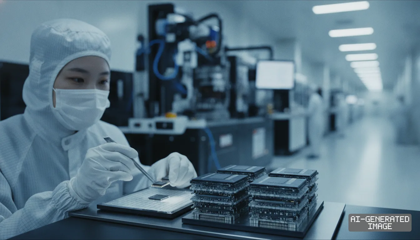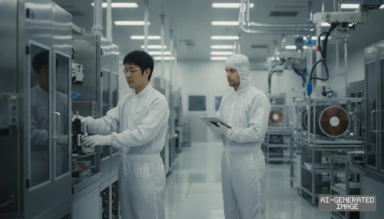
TSMC partners with UC San Diego to train cleanroom engineers
The undergraduate initiative provides more than 200 hours of microfabrication tool training to supply certified fab personnel for TSMC Arizona's $40 billion manufacturing complex in Phoenix.
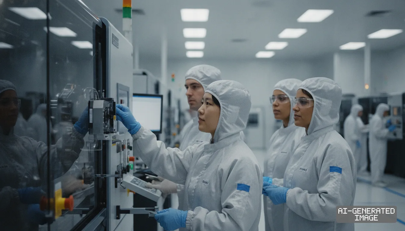
Taiwan Semiconductor Manufacturing Company partnered with the University of California San Diego on Oct. 28, 2026, to establish a specialized undergraduate training program that prepares engineers for cleanroom fabrication roles.
The initiative addresses persistent operational staffing shortages as TSMC prepares its Phoenix manufacturing campus for advanced commercial production. The site requires thousands of trained personnel to operate photolithography, chemical deposition and vacuum machinery.
Under the agreement, the program screens 40 applicants during an introductory fabrication bootcamp and selects 25 students for specialized cleanroom certification. Those 25 students gain direct pipelines to apply for engineering internships at TSMC Arizona.
The training push comes as the wider United States semiconductor manufacturing sector confronts severe workforce constraints. Industry projections indicate that roughly 67,000 technician and engineering positions risk going unfilled across domestic wafer fabrication projects by 2030.
TSMC Arizona operates three planned fabrication facilities in Phoenix representing more than $40 billion in direct capital outlays. The foundry operator expects the Arizona manufacturing hub to create approximately 6,000 direct high-tech positions.
Commercial logic fabrication at advanced nodes requires continuous cleanroom discipline and exacting equipment maintenance. Foundries cannot sustain target wafer yields without certified engineers who understand how chemical delivery, mechanical systems and vacuum chambers interact.
The academic initiative operates through the Center for Memory and Recording Research at the UC San Diego Jacobs School of Engineering. The research center initially tested the curriculum in September 2026 before formalizing the university-level rollout.
Instruction begins during the fall quarter of 2026 with entry-level fabrication exercises. Students work with compact tabletop instruments that reproduce the fundamental physics of deposition, spin-coating and optical patterning at lower operating cost.
The selection process narrows the initial cohort of 40 students down to 25 based on laboratory performance. The successful candidates then transition into the Nano3 Cleanroom Facility operated by UC San Diego's Qualcomm Institute.
Nano3 provides a full-scale microfabrication environment with certified filtration, chemical exhaust lines and commercial-grade wafer tools. Students must complete more than 200 hours of supervised instruction to earn authorization as certified cleanroom operators.
Course organizers structured the curriculum specifically for third-year engineering students. The target cohort draws undergraduates majoring in mechanical engineering, chemical engineering, nanoengineering and chemistry rather than relying solely on conventional electrical engineering programs.
Chip manufacturing demands deep mechanical and chemical proficiency beyond circuit design, program coordinator Oscar Vazquez-Mena said. Foundries rely heavily on specialists who can manage fluid dynamics, reactive gases and complex handling mechanisms on production tools, Vazquez-Mena said.
Faculty members Andrew Kummel, Yu-Hwa Lo and Eric Fullerton direct process development projects alongside cleanroom staff. The coursework emphasizes chemical vapor deposition, wet-chemical etching, atomic layer control and defect inspection protocols used in commercial fabs.
The cleanroom sequence aims to bridge a persistent educational gap across American universities. Most domestic engineering graduates enter software development or device design because few academic institutions operate functional cleanrooms dedicated to undergraduate instruction.
Commercial foundries routinely lose prospective technicians to computing companies that offer remote employment without cleanroom gowning rules or rotating shifts. The hands-on model acclimatizes undergraduate students to physical fabrication environments well before graduation.
The workforce deficit in Phoenix previously disrupted equipment installation timelines during early construction phases. TSMC dispatched hundreds of experienced technicians from its fabrication hubs in Tainan and Hsinchu to support local tooling installation.
Temporary overseas deployments create long-term cost friction and visa complexities for foreign operators. Foundry managers recognized that steady commercial operations require an enduring domestic supply of technicians and process engineers recruited across the American Southwest.
UC San Diego sits within regional reach of major semiconductor manufacturing investments in Southern California and Arizona. The institution graduates hundreds of qualified chemical and materials engineers annually, providing TSMC with a self-sustaining regional recruitment pipeline.
Students who complete the specialized cleanroom coursework will advance into faculty-supervised process projects running from January 2027 through June 2027. That two-quarter project sequence serves as the qualifying threshold for summer 2027 manufacturing internships in Phoenix.
TSMC headquarters has not filed a public disclosure regarding the agreement on the Taiwan Stock Exchange or the U.S. Securities and Exchange Commission, and the university notice did not disclose the total corporate financial contribution.
The academic center will complete evaluations for the pilot cohort at the end of the fall academic quarter in December 2026. The 25 selected undergraduates will then enter the Nano3 cleanroom bays to begin advanced tool authorization.
Impact map
How this development propagates across the region and out to global buyers.
| Event | Korea | China | Japan | Global impact |
|---|---|---|---|---|
| TSMC cleanroom workforce pipeline | Samsung Austin and Taylor fabs compete for the same regional engineering pool | domestic foundries accelerate campus training to counter talent shortages | TSMC Kumamoto fabs rely on Kyushu university consortium for fab engineers | US logic fab operator shortages pose execution risks for multi-billion advanced nodes |
In this story
- Companies
- Taiwan Semiconductor Manufacturing Company
- Tickers
- 2330.TWTSM
- Impact
- Cost StructureCapex
Related briefings
- SK hynix and foundries advance hybrid bonding for AI silicon in 2027 Also on Taiwan Semiconductor Manufacturing Company, Cost Structure
- Lasertec ships EUV pellicle defect inspection tools for sub-2nm chip production Also on Taiwan Semiconductor Manufacturing Company, Cost Structure
- Foundries Standardize 300mm Silicon Photonics PDKs for AI Optical Interconnects Also on Taiwan Semiconductor Manufacturing Company, Cost Structure
- Ibiden and Shinko ramp high-layer FC-BGA lines as AI server package sizes expand Also on Taiwan Semiconductor Manufacturing Company, Cost Structure
Sources
Reporting
Confidence: medium — how we grade this
The documents behind this briefing are linked above. East Asia Brief produces its English text with AI assistance under human editorial review, and does not translate or republish other outlets' articles. See our methodology and AI policy. Spotted an error? Tell us.
The Morning Brief
What changed in Korean, Chinese and Japanese industry overnight — and what it means for your supply chain. One email, weekday mornings, US time. Free.
The Morning Brief is in preparation. Leave your address and we will write to you once — when the first issue is ready. Nothing before that.