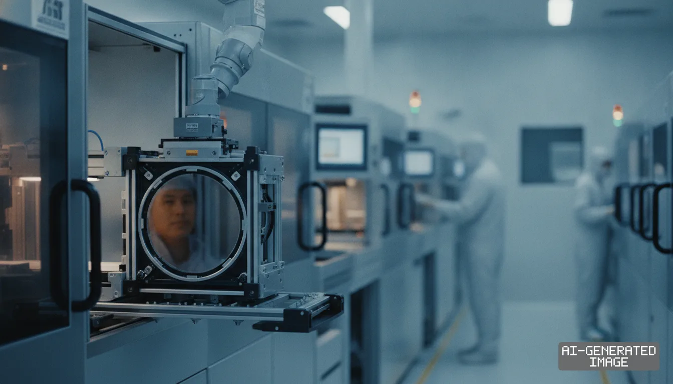
Samsung Foundry debuts 8LPU+ process for automotive chips
The refined deep ultraviolet platform reduces power consumption by 15% and logic area by 8%, giving carmakers an alternative to costlier extreme ultraviolet wafer production lines.

Samsung Electronics introduced its 8LPU+ foundry process on Oct. 23, 2026, upgrading its mature deep ultraviolet lithography platform to capture automotive and edge artificial intelligence chip orders.
The second-generation 8-nanometer node delivers a 12% computing performance increase and a 15% reduction in power consumption compared to the baseline 8LPU process. It also shrinks logic circuit area by 8%.
Samsung Foundry fabricates about 30% of its contract wafer volume on legacy production nodes above 5 nanometers. The upgraded node uses existing argon fluoride immersion tools, avoiding extreme ultraviolet machinery.
Deep ultraviolet lithography tools operate on fully depreciated production lines across the company's Giheung and Hwaseong campuses in South Korea. This established equipment base sharply lowers mask and development overhead for fabless customers.
Extreme ultraviolet scanners produced by Dutch equipment vendor ASML cost more than 200 billion won ($145 million) per unit. Chipmakers operating those tools must pass substantial capital depreciation costs directly onto their wafer purchasers.
Samsung developed its initial 8-nanometer low-power plus technology in 2017 as a refinement of its 10-nanometer platform. The semiconductor maker later introduced its ultimate performance variant, designated 8LPU, in 2018.
The newly detailed 8LPU+ architecture integrates native 3.3-volt planar input-output devices directly onto FinFET wafers. This physical layout reduces peripheral interface circuit area by about 10%, according to conference documentation.
Samsung engineers added ultra-low-leakage static random-access memory and custom high-threshold-voltage transistors to the platform. These circuit elements suppress standby leakage current during idle periods in battery-powered edge devices.
Argon fluoride immersion lithography operates at a 193-nanometer light wavelength, utilizing multi-patterning techniques developed over a decade of high-volume manufacturing. The optical technique eliminates the expensive pellicles and vacuum systems required by extreme ultraviolet tools.
The platform conforms to AEC-Q100 Grade 1 automotive reliability specifications. That automotive standard certifies integrated circuits to withstand continuous thermal operating conditions ranging between minus 40 and 125 degrees Celsius.
Samsung embedded magnetic random-access memory directly into the logic die for automotive grade 1 applications. The non-volatile memory cell achieves a bit area of 0.017 square micrometers, delivering a density near 20 megabits per square millimeter.
Automakers are overhauling vehicle electrical architectures by replacing dozens of distributed electronic control units with centralized zone controllers. Zone controllers consolidate sensor telemetry and actuate physical subsystems within designated physical sectors of a vehicle.
These zonal controllers require upgraded processing throughput to execute real-time machine learning models. Automakers and Tier-1 suppliers reject the high wafer costs and heat generation associated with 3-nanometer or 2-nanometer gate-all-around nodes.
Taiwan Semiconductor Manufacturing Co. manufactures roughly 70% of global automotive microcontrollers on 16-nanometer and 28-nanometer specialty lines. TSMC has also qualified automotive customers on its 7-nanometer FinFET nodes.
Specialty foundries including United Microelectronics Corp. and GlobalFoundries compete aggressively for mature embedded memory sockets. Samsung intends to undercut rival 12-nanometer and 7-nanometer wafer contract pricing by leveraging mature 8-nanometer yields.
Industrial robotics and smart surveillance appliances represent additional expansion targets for the node. Autonomous mobile robots in automated warehouses need on-device neural processing while working within strict battery draw limits.
Edge devices running 8-bit integer quantization models require sustained clock speeds without thermal throttling. The 8LPU+ platform provides the thermal dissipation margins needed for fanless industrial enclosures.
Samsung has accumulated eight years of manufacturing yield data across its 8-nanometer fabrication lines. That operating history gives circuit designers predictable defect densities, preventing sudden yield fallout during initial commercial production runs.
The foundry relies on electronic design automation partnerships to smooth migration for medium-sized fabless firms. Synopsys supplies pre-characterized physical design libraries and embedded memory compilers for the 8LPU+ platform.
Automotive chip qualification cycles typically require two to three years of stress testing before volume deployment. Delivering performance gains on an established node architecture shortens design migration timelines for existing 8-nanometer automotive clients.
Automotive supply chain managers have enforced multi-fab sourcing policies following pandemic-era microcontroller supply shocks. Samsung positions its South Korean 300-millimeter fabs as a viable geographic hedge against concentration risks in Taiwan.
The manufacturing platform illustrates Samsung's dual-track foundry strategy. The company is investing heavily in 2-nanometer gate-all-around development while extracting dependable cash flow from fully amortized mature wafer lines.
Global foundry utilization rates for mature 300-millimeter production capacity softened earlier this year. Introducing specialized automotive and edge AI process features helps backfill fab line utilization without requiring fresh lithography scanner purchases.
The conference abstract does not identify initial commercial tape-out customers, and Samsung has not released pricing schedules for 8LPU+ production wafers.
Samsung will present the complete technical documentation for Paper 3-6 at the IEEE International Electron Devices Meeting in San Francisco on Dec. 14, 2026.
Impact map
How this development propagates across the region and out to global buyers.
| Event | Korea | China | Japan | Global impact |
|---|---|---|---|---|
| Samsung 8LPU+ node rollout | Samsung Foundry expands mature 300mm fab utilization at Giheung and Hwaseong | Domestic auto MCU designers face tougher export pricing from Korean 8nm lines | Renesas and Tier-1 suppliers gain alternative 300mm foundry capacity outside Taiwan | Automotive ZCU bill of materials drops on lower mask costs versus 7nm EUV |
| Samsung 8LPU+ node rollout | Samsung Foundry expands mature 300mm fab utilization at Giheung and Hwaseong | Domestic auto MCU designers face tougher export pricing from Korean 8nm lines | Renesas and Tier-1 suppliers gain alternative 300mm foundry capacity outside Taiwan | Automotive ZCU bill of materials drops on lower mask costs versus 7nm EUV |
In this story
- Companies
- Samsung Electronics
- Tickers
- 005930.KS
- Exposed
- TSMCASMLSynopsys
- Impact
- CapexCost StructurePricing
Related briefings
- Rapidus holds 2nm chip timeline as 17 partners join network Also on Synopsys, TSMC, Samsung Electronics
- Synopsys certifies TSMC A14 EDA flows and tapes out 64G UCIe Also on Synopsys, TSMC, Samsung Electronics
- Rapidus forms 17-firm design alliance to back 2nm chip ramp Also on Synopsys, TSMC
- Synopsys expands TSMC pact with agentic AI chip design tools for A14 Also on Synopsys
Sources
Reporting
Confidence: medium — how we grade this
The documents behind this briefing are linked above. East Asia Brief produces its English text with AI assistance under human editorial review, and does not translate or republish other outlets' articles. See our methodology and AI policy. Spotted an error? Tell us.
The Morning Brief
What changed in Korean, Chinese and Japanese industry overnight — and what it means for your supply chain. One email, weekday mornings, US time. Free.
The Morning Brief is in preparation. Leave your address and we will write to you once — when the first issue is ready. Nothing before that.