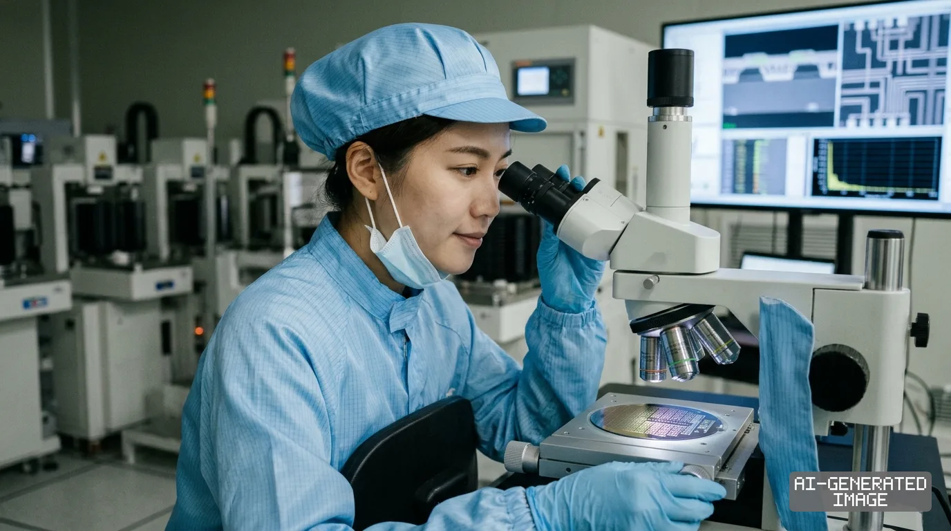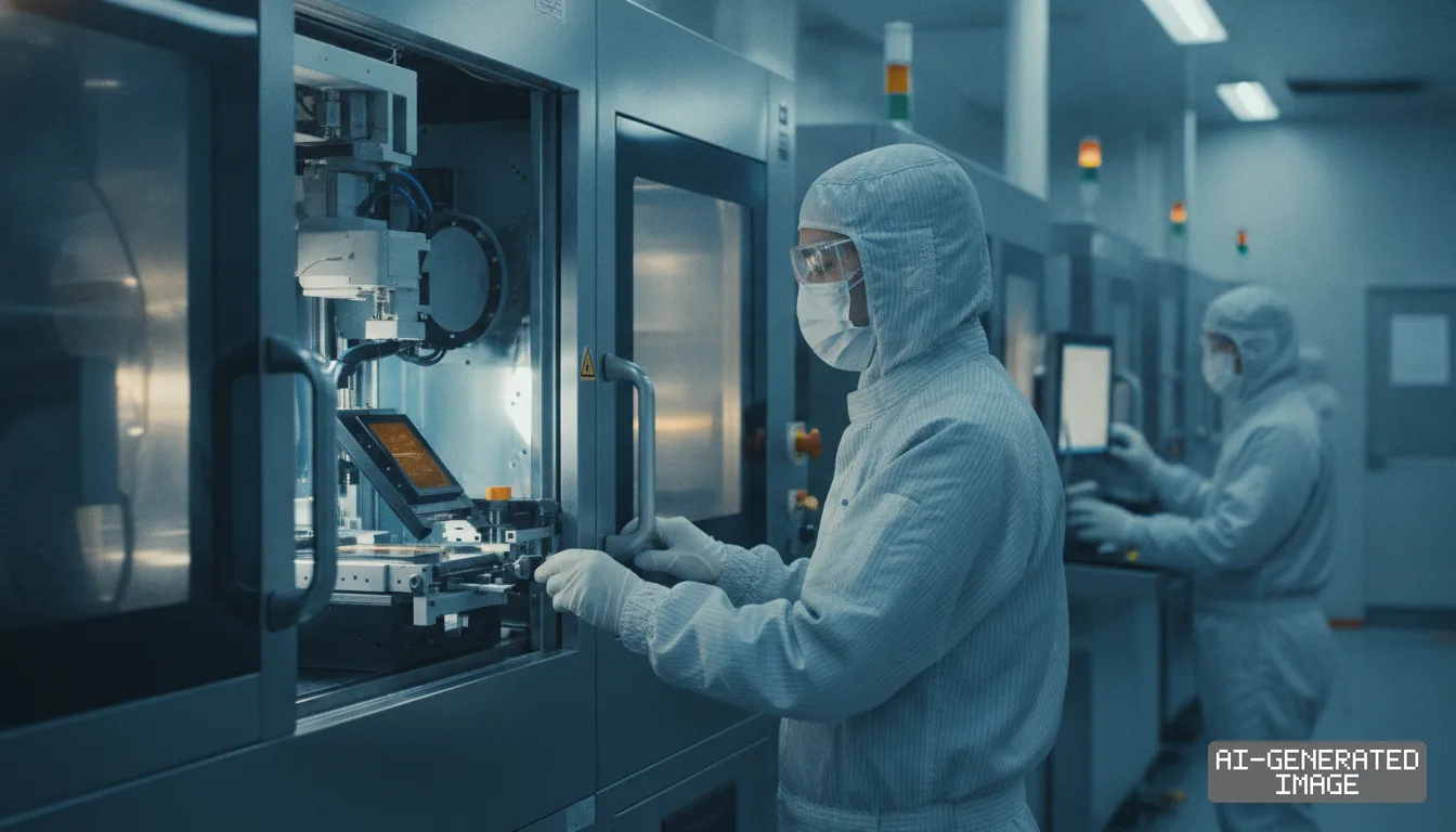
Mirtech begins SK hynix qualification for 300mm wafer tools
The defect inspection specialist aims to break foreign tool dominance across advanced memory lines, targeting 250 billion won in revenue after 2030.
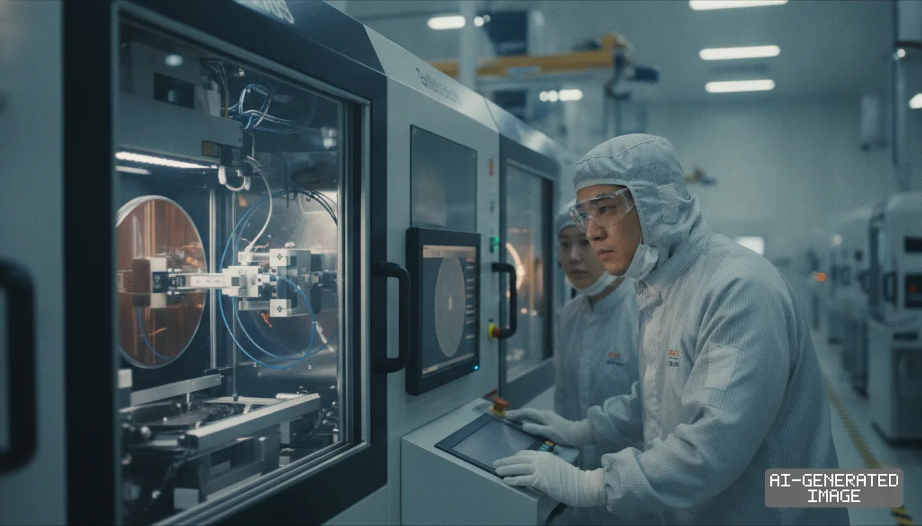
South Korean inspection specialist Mirtech entered commercialization talks with SK hynix on Nov. 20, 2026, following successful qualification of its 300-millimeter full-wafer defect inspection system.
The talks center on qualifying the equipment for commercial memory fabrication lines. Foreign equipment vendors control more than 90% of South Korea's wafer defect inspection tool market, leaving domestic equipment builders with less than 10%.
South Korea's domestic semiconductor inspection and analysis equipment market is projected to expand from 6.7 trillion won ($4.8 billion) in 2026 to 19.3 trillion won by 2035. Mirtech targets annual revenue of 250 billion won ($180 million) after 2030, up from 2.35 billion won ($1.7 million) recorded in 2025.
Conventional fabrication plants rely on sampling metrology tools that inspect less than 3% of processed wafers. Those standalone inspection stations require 10 to 30 minutes per cassette, allowing unspotted macro defects to travel through successive deposition and etching stages.
Yield loss cascades rapidly in high-bandwidth memory (HBM) production. Stacking eight to 16 DRAM dies means a single microscopic flaw on one substrate ruins an entire multi-layer assembly.
Mirtech developed an inline optical inspection module called the IVS series to capture substrate flaws across all processed disks. The hardware mounts directly inside the Equipment Front End Module (EFEM) — the enclosed robotic loader that transfers wafers into processing chambers.
Mounting the scanner inside the transfer unit eliminates the need for separate cleanroom footprint. The optical head scans the entire surface of 150-millimeter, 200-millimeter and 300-millimeter wafers in one to two seconds while the internal robot arm moves, the company said.
The scanner conducts comparative pre-process and post-process imaging on every wafer. Algorithms compare the surface state before and after each fabrication run to pinpoint exactly which chamber caused contamination or scratches, the company said.
Park Jeong-ok founded Mirtech on Jan. 14, 2022, after working 33 years as an equipment and metrology engineer at SK hynix. The venture began inside SK hynix's internal incubation program, known as Hi-Garage, in March 2021.
Mirtech proved the mechanical durability of its inline system in commercial foundry operations before approaching memory fabs. Pure-play foundry operator DB HiTek installed Mirtech's inline inspection tools on 200-millimeter production lines in May 2024 to monitor chemical mechanical planarization (CMP) — a polishing step that flattens wafer surfaces.
The startup also engineered an automated deprocessing unit called WaferoTech. The tool strips individual circuit layers from defective dies to expose physical failure points inside multi-layer structures.
Conventional failure analysis relies on manual chemical etching and mechanical polishing, taking up to 48 hours per specimen. Mirtech's deprocessing tool automates delayering in a single chamber, completing pattern analysis in 30 minutes to two hours, according to company specifications.
South Korean government agencies backed the inspection hardware through several venture commercialization programs. The Ministry of SMEs and Startups selected Mirtech for its DeepTech TIPS program in August 2024, matching 300 million won from venture backer LowPartners with 1.5 billion won in state research grants.
Korea Credit Guarantee Fund designated Mirtech for its First Penguin startup support program in May 2026. The SME ministry also placed the company on its national commendation review list in October 2026, citing its role in developing domestic inspection tools priced at 500 million to 600 million won ($360,000 to $430,000) to replace imported foreign platforms priced at several billion won.
Market dominance in optical defect inspection rests primarily with California-based KLA Corporation, which controls more than 50% of the global semiconductor process control sector. Memory makers seeking to curb capital expenditure have pressed equipment suppliers for lower-cost inline alternatives.
Domestic adoption of inline inspection tools alters fab economics by shifting defect discovery from backend electrical testing to frontend manufacturing. Detecting wafer scratches immediately after chemical polishing prevents fabs from depositing high-cost metal layers onto ruined silicon.
SK hynix and Mirtech plan to conclude technical qualification reviews ahead of commercial mass-production tool installations scheduled for 2027.
The companies have not disclosed final purchase order volumes, tool delivery timetables or total contract values for the planned 2027 deployment.
Impact map
How this development propagates across the region and out to global buyers.
| Event | Korea | China | Japan | Global impact |
|---|---|---|---|---|
| 300mm inline full-wafer inspection deployment | SK hynix cuts scrap costs across advanced DRAM and HBM lines; DB HiTek operates CMP inline units | Domestic foundries remain reliant on imported sampling metrology tools | Tool suppliers face cost pressure from integrated EFEM metrology modules | Inline inspection cuts advanced memory yield-loss cycle from days to minutes |
In this story
Track every Subsidies development →
Related briefings
- East Asia accelerates 8-inch silicon carbide capacity race as power chip makers scale output Also on DB Hitek, Subsidies, Cost Structure
- Samsung Foundry converts mature planar lines to automotive power chips Also on DB Hitek, Subsidies, Cost Structure
- US chip controls threaten Nvidia's $5B compound power plan for AI centers Also on DB Hitek, Subsidies
- Korea Foundries Shift 200mm Lines to Auto PMICs as EV Architectures Advance Also on DB HiTek, Subsidies
Sources
Primary documents
Reporting
Confidence: high — how we grade this
The documents behind this briefing are linked above. East Asia Brief produces its English text with AI assistance under human editorial review, and does not translate or republish other outlets' articles. See our methodology and AI policy. Spotted an error? Tell us.
The Morning Brief
What changed in Korean, Chinese and Japanese industry overnight — and what it means for your supply chain. One email, weekday mornings, US time. Free.
The Morning Brief is in preparation. Leave your address and we will write to you once — when the first issue is ready. Nothing before that.