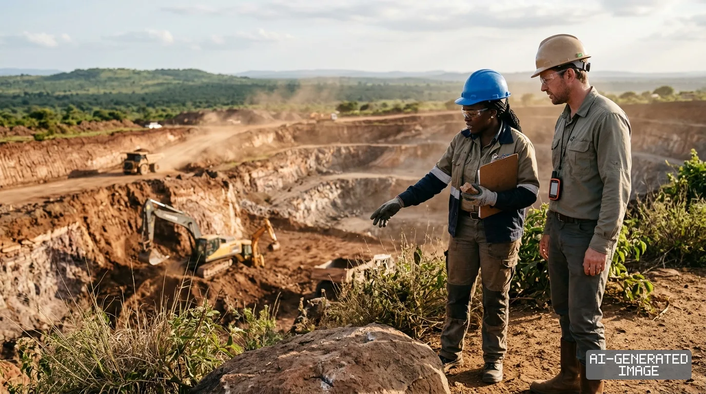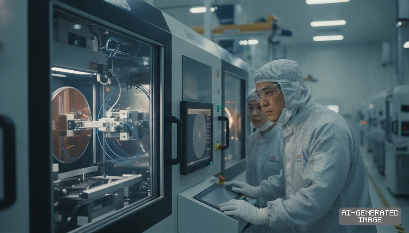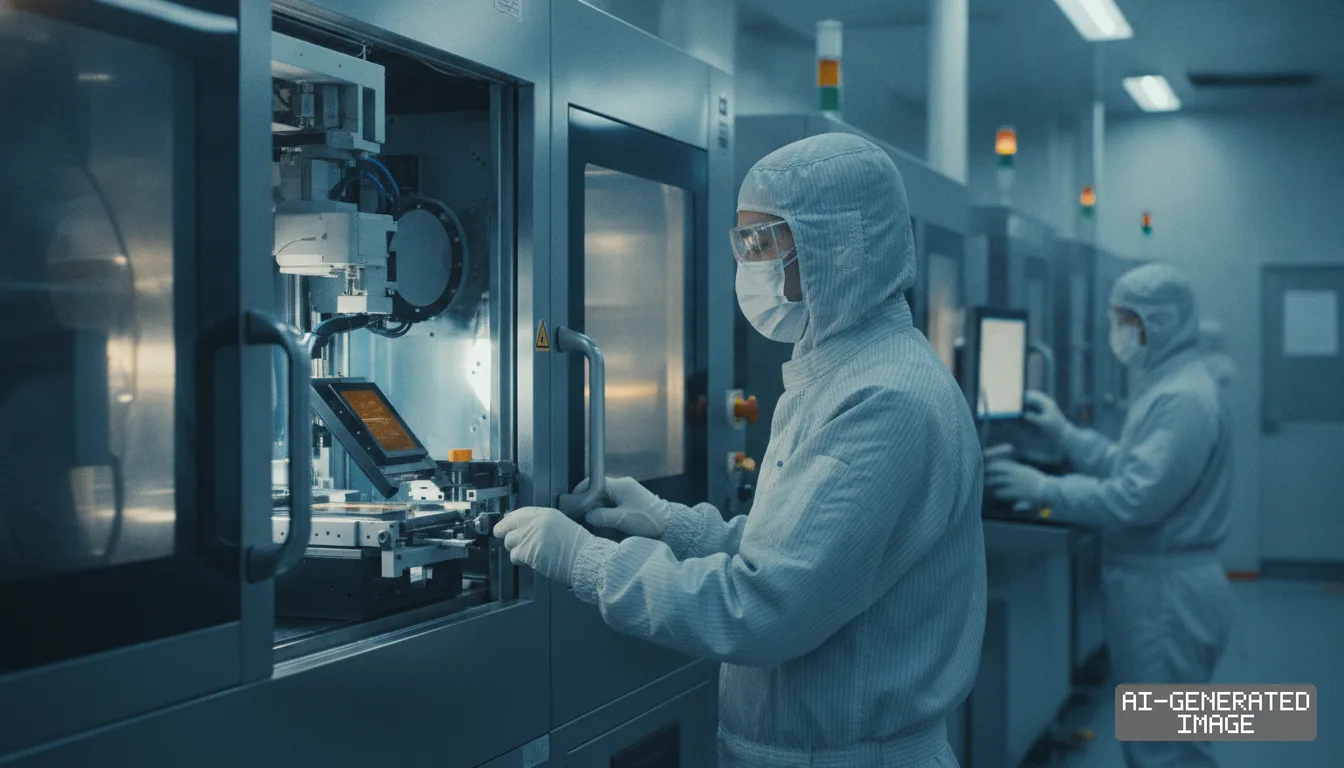
Apple deploys TSMC hybrid bonding on M5 chips to multiply density
A chip teardown shows sub-10-micrometer copper bonding replacing solder microbumps across the M5 family, as Apple generates roughly 25% of TSMC foundry revenue.
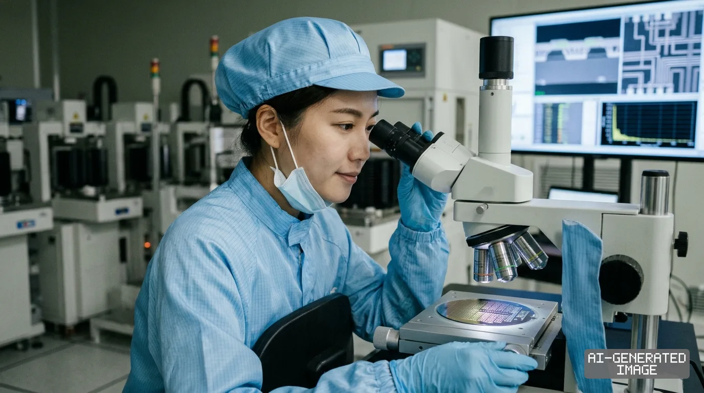
Taiwan Semiconductor Manufacturing Co. deployed copper-to-copper hybrid bonding across Apple's M5 processor family, lifting interconnect density sixfold in a chip-level teardown published Nov. 20, 2026.
The interconnect shrinks bond pitch below 10 micrometers, replacing conventional 25-micrometer solder microbumps. That reduction multiplies the physical connection paths linking separated processor dies, the teardown report showed.
Apple accounts for roughly 25% of TSMC's foundry revenue, making the packaging transition a high-volume anchor for the foundry's advanced packaging lines. TSMC generated 46% of its revenue from high-performance computing platforms in early 2026.
The teardown established that Apple split the M5 architecture into modular chiplets rather than manufacturing a single monolithic silicon die. A dedicated central processing unit die measures roughly 168 square millimeters across 18 cores.
Graphics processing units sit on separated dies, divided into scaled variants of about 300 square millimeters and 157 square millimeters. Splitting logic into smaller dies lifts manufacturing yields and bypasses reticle limits near 830 square millimeters.
TSMC calls the underlying packaging process System-on-Integrated-Chips with molded horizontal assembly, or SoIC-mH. The method joins silicon dies face to face without solder, fusing copper pads and surrounding dielectric materials under heat and pressure.
Apple brands the high-speed bridge between dual dies as UltraFusion. In earlier processors like the M3 Ultra, UltraFusion relied on solder microbumps over silicon interposers to connect paired system-on-chip units into a unified desktop processor.
Solder microbumps encounter electrical resistance and signal delays as bond pitches contract below 10 micrometers. Copper-to-copper hybrid bonding eliminates the solder alloy, allowing direct metal contact that reduces parasitic capacitance and cuts transmission energy.
The teardown analysis reconstructed the M5 Ultra interconnect structure by examining physical test interfaces found on retail M5 Pro and M5 Max hardware. Engineers measured pad dimensions and cross-referenced the layout against official system performance disclosures.
Apple Support released technical specifications and repair manuals for M5-powered Mac Studio models in September 2026. Those documents verified unified memory bandwidth reaching 1.2 terabytes per second, while omitting vendor names and packaging specifications.
Reverse-engineering laboratory TechInsights had confirmed TSMC hybrid bonding on earlier M5 Pro engineering samples on June 30, 2026. The latest teardown provides the first public confirmation of horizontal die integration across the full desktop silicon family.
The shift deepens Apple's reliance on TSMC's proprietary packaging platform, reinforcing a competitive barrier against foundry competitors. Intel and Samsung Electronics have struggled to match the commercial scale of TSMC's integrated wafer fabrication and packaging network.
Intel deployed hybrid bonding with its Foveros Direct packaging at a 9-micrometer pitch for Clearwater Forest server processors earlier in 2026. However, Intel has yet to demonstrate volume manufacturing across consumer client personal computers.
Samsung Electronics has promoted its own Saint 3D stacking processes for high-bandwidth memory, but the company has not secured tier-one client processor volume for logic-on-logic hybrid bonding. That leaves TSMC holding an effective production monopoly in commercial client chiplets.
Advanced packaging capacity remains tightly allocated at TSMC's domestic fabrication facilities in Taiwan. Expanding hybrid bonding requires cleanroom environments matching frontend wafer lithography standards, which raises capital expenditure per square meter of backend manufacturing floor space.
The capital intensity limits advanced packaging access to high-margin products like artificial intelligence accelerators and flagship personal computers. Standard mobile application processors continue to rely on lower-cost integrated fan-out packaging technologies.
TSMC's published technology roadmap targets a tighter 4.5-micrometer hybrid bonding pitch by 2029. The foundry plans to pair that pitch reduction with two-nanometer logic nodes to serve next-generation artificial intelligence accelerators and workstation processors.
The physical teardown does not include a direct cross-section measurement of an M5 Ultra retail package, and neither Apple nor TSMC has published the bonding pitch specifications in regulatory filings.
The teardown findings show that advanced packaging has supplanted traditional node shrinking as the primary driver of computing density, cementing TSMC's position across Apple's high-performance hardware lineup.
Impact map
How this development propagates across the region and out to global buyers.
| Event | Korea | China | Japan | Global impact |
|---|---|---|---|---|
| Apple M5 hybrid bonding adoption | Samsung Electronics lacks client logic hybrid bonding orders | Domestic foundries remain locked out of sub-10um hybrid bonding lines | Equipment vendors Tokyo Electron and DISCO capture hybrid bonding tool spend | TSMC widens packaging lead as client processors adopt chiplet bonding |
In this story
- Companies
- AppleTSMC
- Tickers
- AAPL2330.TW
- Exposed
- IntelSamsung Electronics
- Impact
- Supply ChainCapex
Related briefings
- TSMC secures $30,000 wafer rate, while Rapidus slips on 2nm ramp Also on Apple, Intel, Samsung Electronics
- TSMC warns AI cannot solve physical barriers for 1.4nm chips Also on Apple, Intel, Samsung Electronics
- TSMC Reaffirms 2028 Target for 1.4nm Chips at Taichung Fab Also on Apple, Intel, Samsung Electronics
- TSMC sees 3nm revenue overtake 5nm node on surge in AI accelerators Also on Apple, Intel, Samsung Electronics
Sources
Primary documents
Reporting
Confidence: high — how we grade this
The documents behind this briefing are linked above. East Asia Brief produces its English text with AI assistance under human editorial review, and does not translate or republish other outlets' articles. See our methodology and AI policy. Spotted an error? Tell us.
The Morning Brief
What changed in Korean, Chinese and Japanese industry overnight — and what it means for your supply chain. One email, weekday mornings, US time. Free.
The Morning Brief is in preparation. Leave your address and we will write to you once — when the first issue is ready. Nothing before that.