Lam Research builds $300m Taiwan R&D center for TSMC sub-2nm chips
The 40,000-square-meter Zhunan facility expands cleanroom space ninefold by 2028 to co-develop etch and deposition tools with TSMC.
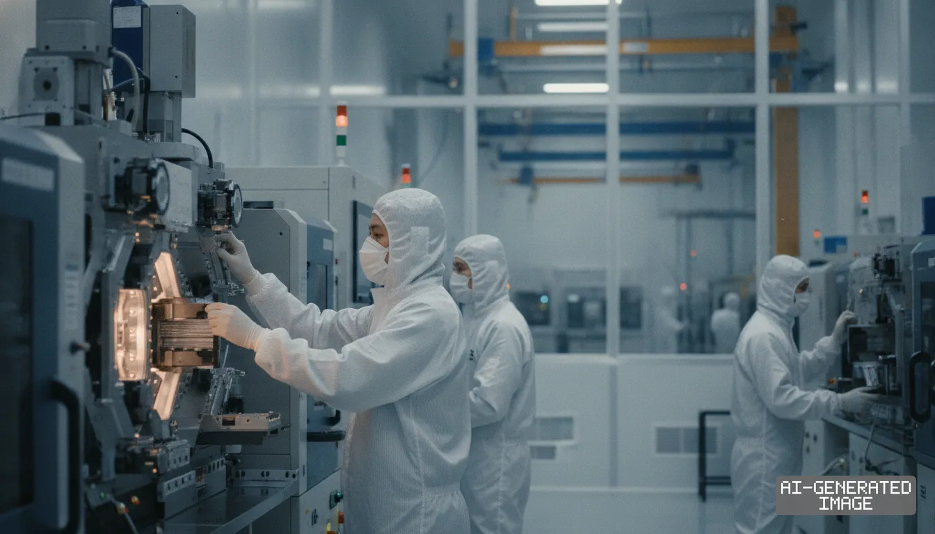
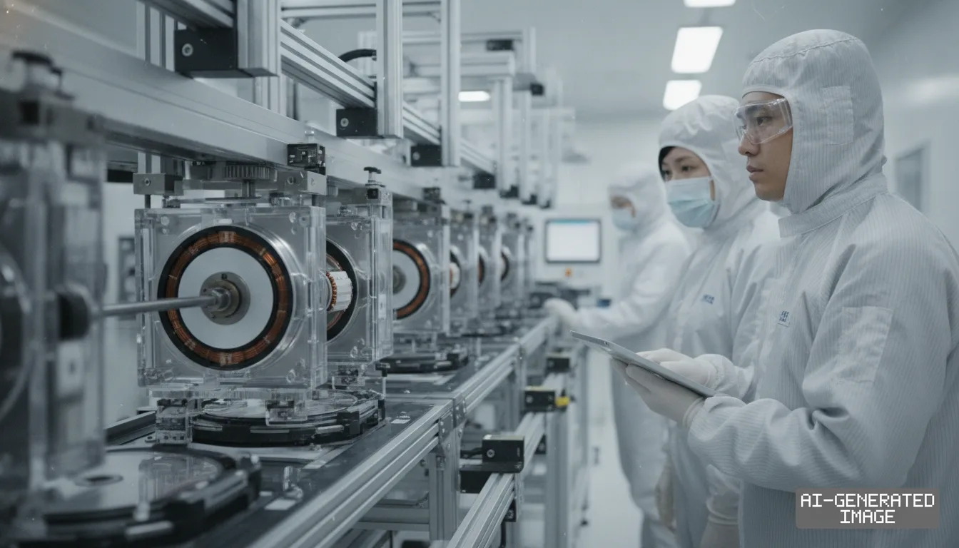
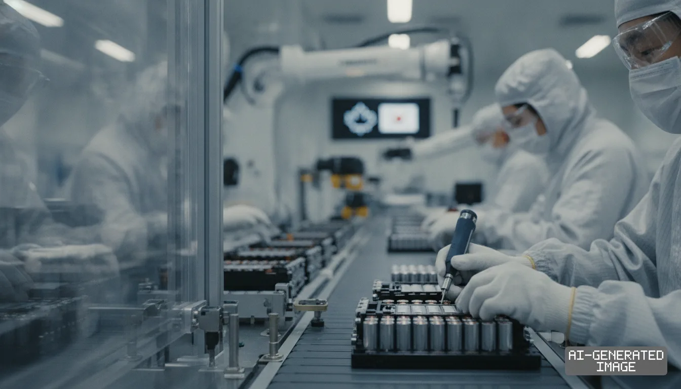
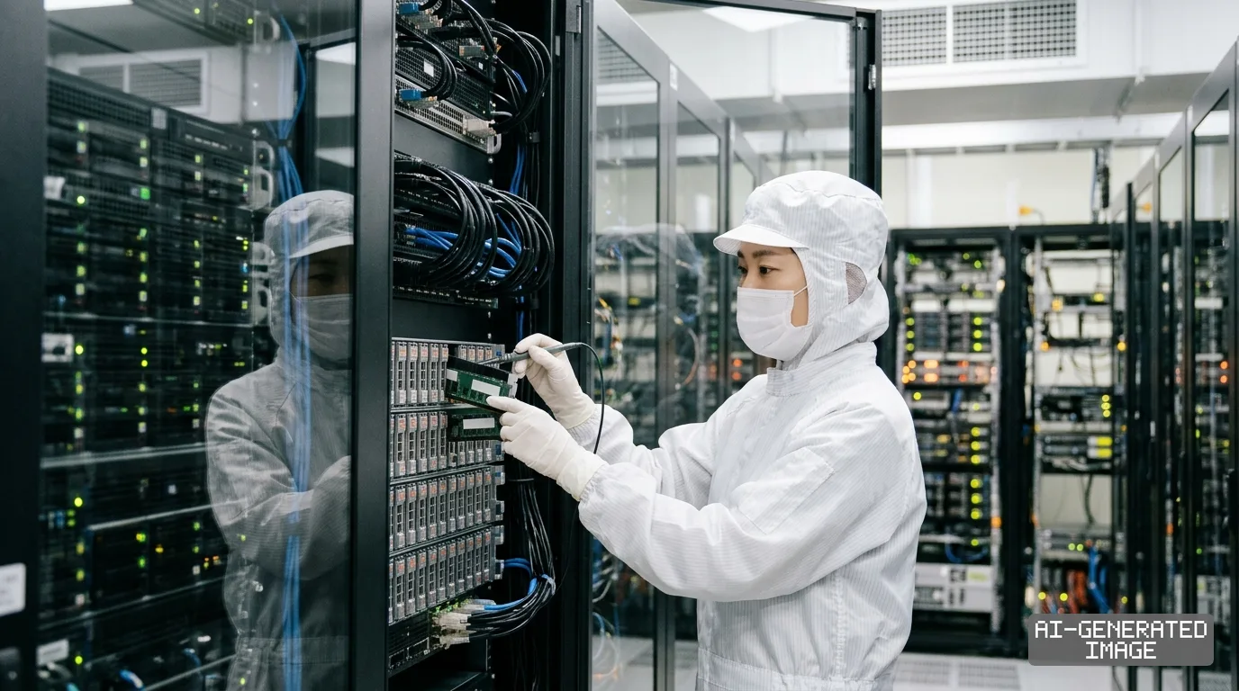
Lam Research broke ground Nov. 19, 2026, on a $300 million technology center in Miaoli County, Taiwan, expanding cleanroom space to accelerate sub-2-nanometer etch and deposition development with TSMC.
The Zhunan facility spans more than 40,000 square meters of office and cleanroom space. The site will expand the company's laboratory footprint in Taiwan roughly ninefold when it opens in 2028.
The $300 million outlay accounts for 10% of the five-year, $3 billion global research network expansion Lam Research announced on Aug. 13. The company is funding the program from operating cash flow.
Lam Research Chief Operating Officer Sesha Varadarajan and TSMC co-Chief Operating Officer Y.J. Mii attended the ceremony. Both companies committed to shortening verification cycles for next-generation transistor structures.
The joint work will focus on selective etch, chemical deposition, wet clean and advanced packaging tools. The program targets logic nodes below 2 nanometers using gate-all-around architectures, where microscopic ribbons require atomic precision.
Foundries are transitioning from FinFET transistors to gate-all-around designs, which wrap conductive gates entirely around horizontal silicon nanosheets. That architectural shift requires three to five times more atomic layer deposition steps than older nodes.
Etching those nanosheet stacks demands selective gas chemistry that strips sacrificial layers without eroding silicon channels. Process engineers must adjust plasma frequency and wafer temperature in real time alongside foundry technicians.
The research site will also develop tools for backside power delivery networks, which move power rails to the wafer rear. That architecture requires deep through-silicon etching and precise planarization to prevent wafer warpage.
Microscopic residue removal presents another yield hurdle as feature dimensions drop below 2 nanometers. Lam Research wet clean systems will target sub-10-nanometer particle removal without causing fragile nanosheet channels to collapse.
Zhunan sits directly along Taiwan's northern semiconductor corridor between Hsinchu and Taichung. Placing process laboratories minutes from TSMC pilot lines eliminates weeks of shipping developmental wafers back and forth across the Pacific.
The site also borders TSMC's Advanced Backend Fab 6 in Zhunan. That proximity supports engineering work on 3D wafer stacking and chip-on-wafer packaging used in high-bandwidth artificial intelligence accelerators.
Advanced packaging now requires front-end wafer fabrication techniques as interconnect pitches shrink to single microns. Lam Research is deploying specialized dielectric etch and copper barrier deposition systems to support those high-density packaging lines.
Taiwan represents one of Lam Research's two primary geographic revenue drivers alongside South Korea. Together, the two markets generated over 50% of the equipment maker's $23.23 billion in fiscal 2026 revenue.
Global semiconductor equipment billings reached $135.1 billion in 2025, according to SEMI trade data. Taiwan absorbed $31.5 billion of that total, up 90% year over year on aggressive advanced-node capacity expansion.
Co-developing process recipes at early research stages creates durable tool-of-record lock-in for equipment makers. Once a foundry qualifies a specific etch chamber for mass production, replacing that tool carries prohibitive yield risk.
The Zhunan expansion tightens Lam Research's grip on TSMC's leading-edge tool list. The foundry relies on foreign equipment vendors for more than 85% of its wafer fabrication machinery.
TSMC recognized Lam Research for technology and production support at its annual supply chain forum on Nov. 17. The award reflected tool uptime and joint engineering performance during initial 2-nanometer pilot installations.
The expanded laboratory footprint sharpens competition against rival toolmakers Applied Materials and Tokyo Electron. All three vendors are competing for high-aspect-ratio dielectric etch and conductor etch slots across Taiwan's foundries.
The facility also widens the technical moat against aspiring Asian toolmakers. While mainland Chinese suppliers expand mature-node market share, they remain entirely excluded from sub-2-nanometer gate-all-around development loops inside Taiwan.
The center will create hundreds of engineering positions in Miaoli County. New hires will include process integration specialists, plasma physicists and hardware engineers tasked with maintaining commercial-scale wafer processing equipment.
Lam Research has not filed an 8-K disclosure with the US Securities and Exchange Commission regarding the capital commitment. Taiwan's Ministry of Economic Affairs has not published details on local subsidy amounts for the site.
Facility construction in Zhunan will continue through 2027. Tool installation and cleanroom certification will follow ahead of commercial operations scheduled for the first half of 2028.
Impact map
How this development propagates across the region and out to global buyers.
| Event | Korea | China | Japan | Global impact |
|---|---|---|---|---|
| Lam Taiwan R&D expansion | Samsung foundry faces tighter equipment vendor alignment at TSMC clusters | Domestic etch toolmakers like AMEC remain excluded from sub-2nm GAA development loops | Tokyo Electron contends with expanded Lam presence across advanced packaging and dry etch | Sub-2nm transistor yields tied closer to co-located wafer fab equipment labs |
In this story
- Companies
- Lam ResearchTSMC
- Tickers
- LRCX2330.TW
- Exposed
- Applied MaterialsTokyo Electron
- Impact
- Supply ChainCapex
Related briefings
- Skytech opens TSMC-backed advanced process lab to speed chip tool verification Also on Lam Research, Applied Materials, Tokyo Electron
- Japan Linear Guide Makers Expand Ultra-Clean Units for 2nm Fab Robotics Also on Lam Research, Applied Materials, Tokyo Electron
- ASML and tool makers see China sales share plunge in third quarter Also on Lam Research, Applied Materials, Tokyo Electron
- Senator Cotton demands US blacklist on CXMT as DRAM share hits 10% Also on Lam Research, Applied Materials
Sources
Primary documents
Reporting
Confidence: high — how we grade this
The documents behind this briefing are linked above. East Asia Brief produces its English text with AI assistance under human editorial review, and does not translate or republish other outlets' articles. See our methodology and AI policy. Spotted an error? Tell us.
The Morning Brief
What changed in Korean, Chinese and Japanese industry overnight — and what it means for your supply chain. One email, weekday mornings, US time. Free.
The Morning Brief is in preparation. Leave your address and we will write to you once — when the first issue is ready. Nothing before that.