YMTC targets 70% domestic tool share for 300-layer Wuhan fab
A planned fourth facility aims to raise local procurement from 50% at its third site to build high-density flash for cloud and AI data centers.
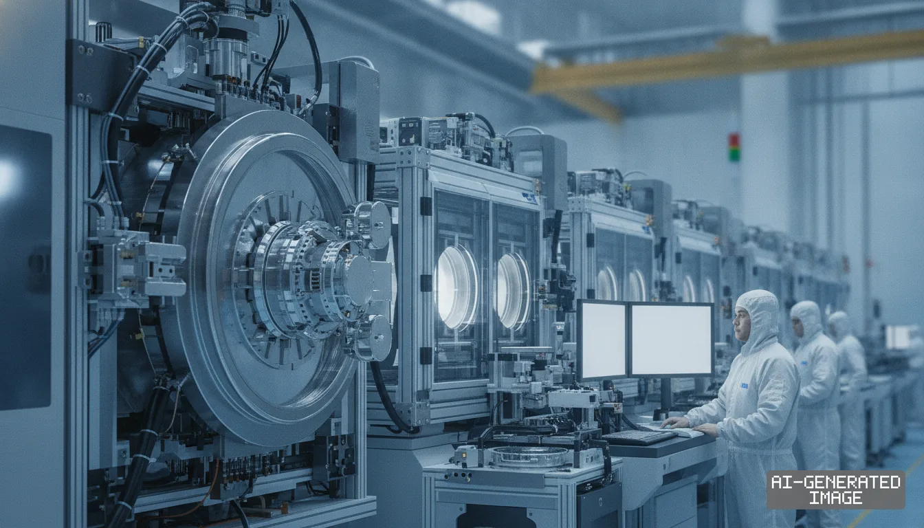
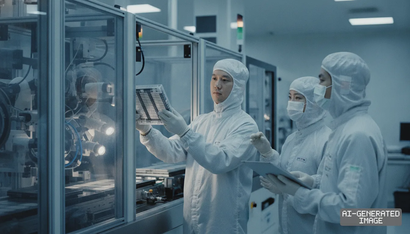
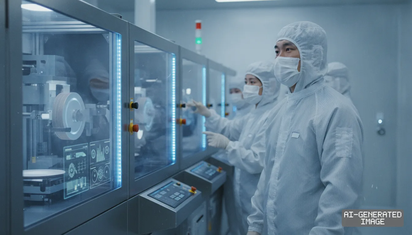
Yangtze Memory Technologies Co. advanced engineering plans on Nov. 7, 2026, to construct a fourth wafer fab dedicated to 300-plus layer NAND flash memory in Wuhan.
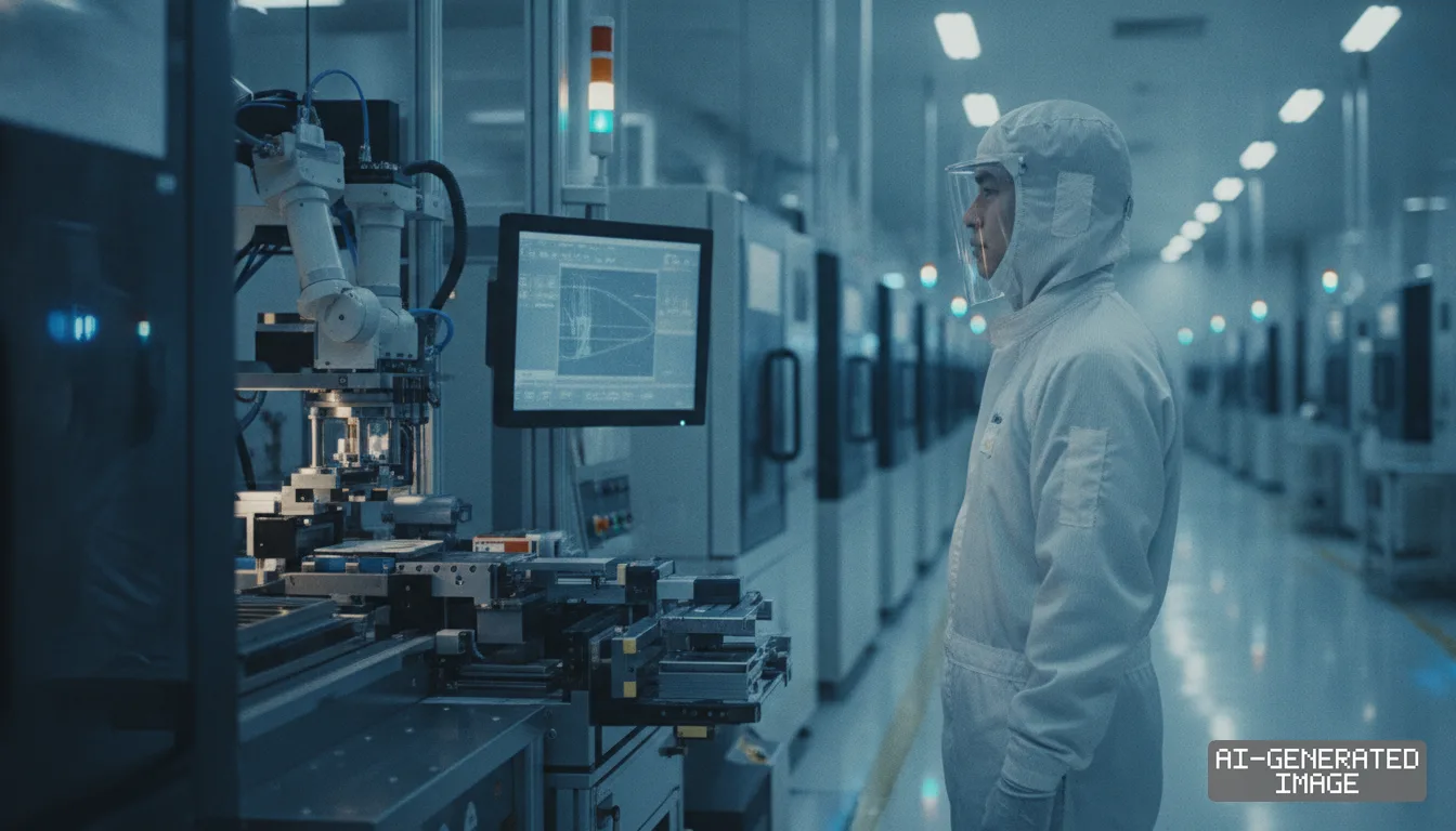
The facility targets a domestic equipment procurement share of at least 60% with an upper objective of 70%, toolmaker personnel said. Chinese suppliers provided just over 50% of the tools installed at YMTC's third Wuhan fab, making the new target an expanded domestic sourcing threshold.
Each manufacturing plant across YMTC's Wuhan campus carries a design capacity of 100,000 wafer starts per month. The fourth factory will focus on producing high-density flash storage chips for hyperscale cloud data centers and artificial intelligence computing workloads.
YMTC held a 38.5% share of China's NAND flash memory market in the second quarter of 2026, rising from 28% across 2025, according to market data compiled by Omdia. The supplier surpassed Samsung Electronics to capture the top volume position in the Chinese flash storage market during that three-month reporting period.
The 300-plus layer architecture relies on YMTC's proprietary Xtacking process, which fabricates peripheral circuits and memory arrays on two separate wafers before bonding them face-to-face. Splitting circuit fabrication across two substrates prevents the high-temperature annealing of memory cells from degrading the CMOS logic below.
The modular bonding technique also limits wafer warpage during the extreme vertical stacking required for high-density flash chips, engineers familiar with the process said. That structural method allows YMTC to pursue higher layer counts despite foreign trade restrictions on single-pass etch tools.
Deep channel hole etching presents the steepest manufacturing hurdle for 300-layer flash memory. Fabricating high-aspect-ratio holes through hundreds of alternating dielectric layers requires precise plasma density control and high radio-frequency power.
The United States Department of Commerce placed YMTC on its Entity List in December 2022, cutting off access to American semiconductor manufacturing gear. Export regulations restrict American shipments of advanced etching and deposition systems configured for NAND fabrication lines exceeding 128 layers.
Those restrictions accelerated equipment qualification for mainland tool vendors. Naura Technology Group and Advanced Micro-Fabrication Equipment, known as AMEC, represent the primary domestic beneficiaries of the fab expansion.
Naura supplies dry etching, oxidation, cleaning and physical vapor deposition equipment, drawing over 70% of its annual tool revenue from mainland Chinese chipmakers. AMEC supplies dielectric etch systems engineered for high-aspect-ratio channel hole patterning.
AMEC tools currently account for roughly 30% of the dry etch equipment installed in YMTC cleanrooms, vendor filings show. Thin-film deposition specialist Piotech and wet-cleaning provider ACM Research also maintain qualified equipment lines at the Wuhan campus.
Domestic orders for the fourth fab will concentrate heavily in wafer cleaning, polishing and dielectric etching stages. Chinese suppliers have achieved high operational stability across those workhorse processing modules.
Overseas toolmakers retain an effective monopoly on deep ultraviolet immersion lithography and optical pattern inspection stations. No Chinese manufacturer produces commercial deep ultraviolet immersion lithography systems capable of sub-28-nanometer pitch patterning at production yields.
Foreign memory producers operating in China face parallel operational limitations from United States export controls. Samsung Electronics operates a twin-fab NAND complex in Xi'an, Shaanxi province, which produces roughly 40% of Samsung's worldwide NAND flash bit output.
Samsung currently upgrades that facility to 286-layer V-NAND under annual Validated End-User authorizations granted by Washington. SK hynix upgrades its Dalian fab toward 240-layer chips under matching export authorizations.
United States trade officials have indicated that annual tool authorizations will not permit capacity expansions or advanced technology jumps at either foreign facility in China. The regulatory ceiling effectively limits output competition from multinational rivals within the Chinese domestic market.
Global NAND flash contract prices experienced steady upward momentum throughout 2026 due to strong enterprise solid-state drive demand from AI server clusters. Expanding domestic flash production shields Chinese server manufacturers, including Inspur and Lenovo, from international memory pricing cycles.
The three newer fabs in Wuhan—numbered three, four and five—will lift YMTC's total monthly capacity beyond 300,000 wafer starts upon completion. That planned volume would double the company's total production base.
Financing for the multi-billion-dollar project follows a filing by YMTC parent entity CCSH Corporation to list on the Shanghai STAR Market. The parent company submitted an application in August 2026 seeking to raise 33 billion yuan ($4.6 billion) for advanced memory line investments.
Prospectus disclosures showed that YMTC's first two Wuhan fabs operated at an aggregate capacity utilization rate of 98.02% during the first half of 2026. CCSH Corporation paused the offering in early November 2026 amid falling stock market valuations and regulatory scrutiny of tech listings.
The company has not published an official engineering notice for the fourth fab, and equipment suppliers confirm that YMTC has not yet issued formal purchase orders for the project. Published regulatory records also do not disclose verified wafer yields for domestic etch tools operating on 300-layer stacks.
Construction on the fourth Wuhan fab is scheduled to break ground in 2027, according to project planners. Initial wafer production at the third Wuhan facility begins before Dec. 31, 2026.
Impact map
How this development propagates across the region and out to global buyers.
| Event | Korea | China | Japan | Global impact |
|---|---|---|---|---|
| YMTC 300-layer NAND fab expansion | Samsung and SK hynix face capped China tool upgrades at Xi'an and Dalian fabs | Naura and AMEC gain tool share while YMTC targets 70% domestic fab equipment | Tokyo Electron and Canon face restricted advanced tool sales to Chinese memory lines | Enterprise SSD capacity increases as Chinese cloud providers shift procurement domestically |
In this story
- Companies
- Yangtze Memory Technologies Co.
- Exposed
- Naura Technology GroupAdvanced Micro-Fabrication EquipmentSamsung ElectronicsSK hynix
- Policy
- Export Controls
- Impact
- Supply ChainCapexPricing
Track every Export Controls development →
Related briefings
- Samsung denies Chinese tool testing as US tightens fab controls Also on Advanced Micro-Fabrication Equipment, SK hynix, Samsung Electronics
- YMTC targets 70% domestic equipment for fourth Wuhan 3D NAND fab Also on Yangtze Memory Technologies Co., Naura Technology Group, SK hynix
- Samsung and SK hynix upgrade China memory fabs to 286 layers Also on Yangtze Memory Technologies Co., SK hynix, Samsung Electronics
- SMIC hits record $9.33B revenue as legacy nodes mask 7nm lag Also on Naura Technology Group, Export Controls, Pricing
Sources
Reporting
Confidence: medium — how we grade this
The documents behind this briefing are linked above. East Asia Brief produces its English text with AI assistance under human editorial review, and does not translate or republish other outlets' articles. See our methodology and AI policy. Spotted an error? Tell us.
The Morning Brief
What changed in Korean, Chinese and Japanese industry overnight — and what it means for your supply chain. One email, weekday mornings, US time. Free.
The Morning Brief is in preparation. Leave your address and we will write to you once — when the first issue is ready. Nothing before that.