Samsung's Lee Jae-yong inspects Yokohama packaging R&D center
The South Korean chipmaker commits ¥40 billion to accelerate wafer bonding and glass substrate trials alongside Japanese equipment and materials partners.
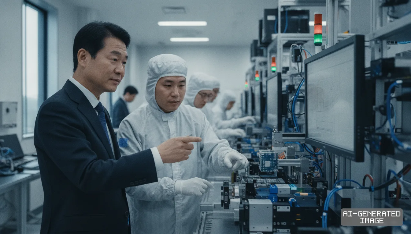
Samsung Electronics Executive Chairman Lee Jae-yong inspected the company's Advanced Package Lab in Yokohama, Japan, on Nov. 1, 2026, ordering closer technical collaboration with local materials and equipment makers.
The visit marks Lee's first on-site inspection of the packaging research base since operations began on Sept. 8. Samsung Electronics is spending ¥40 billion ($254 million) over five years through 2028 to build out the packaging facility.
The 6,600-square-meter facility in Yokohama's Minato Mirai district operates with 95 researchers from South Korea and Japan. Samsung plans to increase the engineering staff to more than 100 researchers by 2027.
Hiroichi Kawahira, vice president and head of Samsung Electronics DS Research Japan, and Takashi Kariya, managing director and head of the Advanced Package Lab, accompanied Lee during the site review, the company said in a notice.
Lee reviewed development milestones for next-generation packaging materials and process technologies with on-site researchers. He urged engineers to secure proprietary packaging architectures necessary for artificial intelligence hardware, the company said.
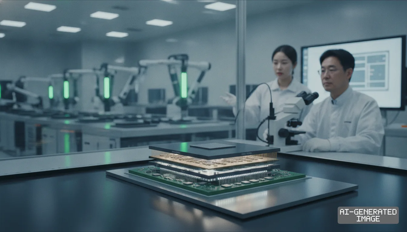
Advanced packaging connects processors and high-bandwidth memory — DRAM stacks that feed data to artificial intelligence accelerators — into a single package. The process shortens signal paths and lowers power consumption during intense computing workloads.
The physical scaling of silicon transistors has slowed as circuit line widths approach atomic limits. Chipmakers now rely on advanced packaging architectures, stacking disparate silicon dies vertically and horizontally, to deliver generational leaps in processor throughput.
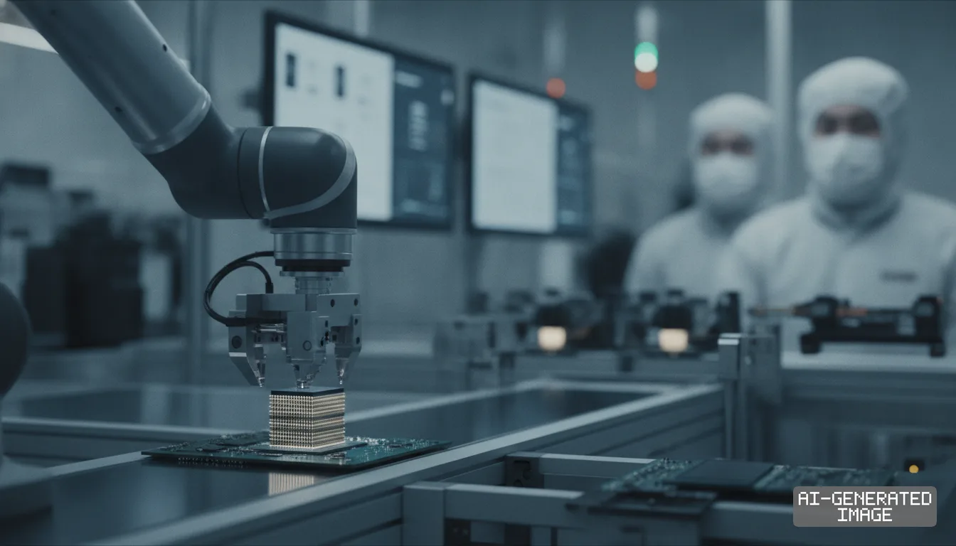
The Yokohama facility focuses on core back-end process technologies, including wafer bonding and glass substrates. Wafer bonding fuses silicon layers directly together, while glass substrates replace organic resin cores to carry denser wiring without warping under heat.
Samsung Electronics aims to validate new package architectures for low-power artificial intelligence accelerators. The company seeks to combine contract chip fabrication, memory production and advanced packaging into a single turnkey service for global artificial intelligence hardware customers.
The Japanese research hub operates separately from the packaging research unit under Samsung's Semiconductor R&D Center in South Korea. The company said the two research units will coordinate to share process recipes and avoid duplicate capital expenditures.
The City of Yokohama cleared the investment on Dec. 21, 2023, approving local corporate subsidies for Samsung to locate the research site in its central business district. Japan's Ministry of Economy, Trade and Industry approved up to ¥22.5 billion in supporting subsidies.
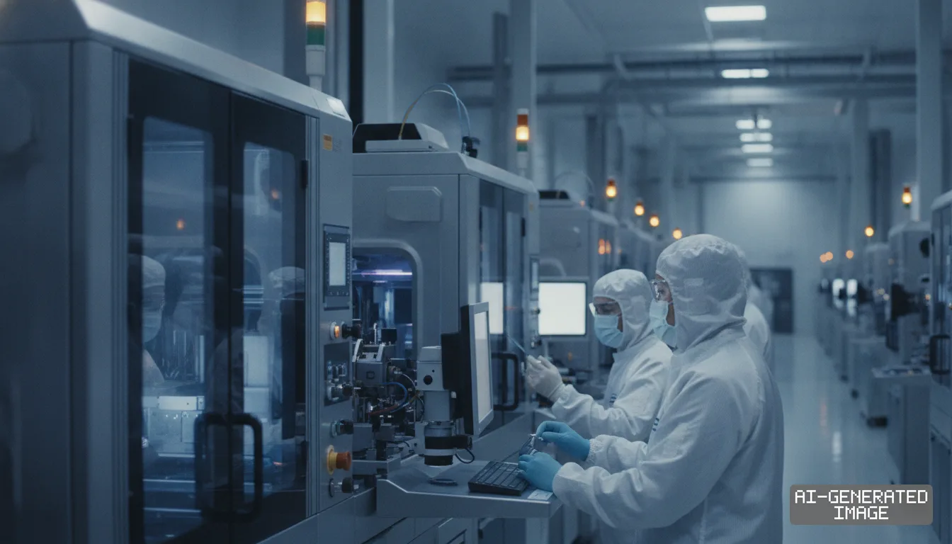
The facility contains a cleanroom engineered to duplicate commercial production line conditions rather than standard laboratory benches. The layout allows engineers to evaluate experimental resins, films and bonding tools under actual manufacturing stress, the company said.
Representatives from 15 Japanese semiconductor supply companies attended the laboratory's opening ceremony in September. Japan's supply chain retains dominant market shares in critical back-end materials, including photoresists, underfills, epoxy molding compounds and high-precision wafer dicers.
Samsung Electronics did not disclose in its announcement the specific Japanese tool and materials suppliers it met with, nor did it confirm any newly signed supply contracts or memorandums of understanding.
Samsung Electronics established its first research office in Japan in 1992 and opened a dedicated facility in Yokohama in 1997. The Advanced Package Lab now operates under its consolidated Device Solutions Research Japan unit.
Samsung will expand the Yokohama packaging lab's engineering headcount past 100 by 2027 while advancing glass substrate and hybrid wafer bonding architecture trials.
Impact map
How this development propagates across the region and out to global buyers.
| Event | Korea | China | Japan | Global impact |
|---|---|---|---|---|
| Yokohama Advanced Package Lab inspection | Samsung aligns memory and foundry arms with Japanese packaging toolmakers | Domestic chiplet packaging efforts face widening technical gap in hybrid bonding | Materials and equipment suppliers secure direct qualification access to Samsung pilot lines | AI chip designers gain second turnkey advanced packaging alternative to TSMC |
In this story
- Companies
- Samsung Electronics
- Tickers
- 005930.KS
- Policy
- Subsidies
- Impact
- CapexSupply Chain
Track every Subsidies development →
Related briefings
- Solidigm weighs $45B US NAND plant as AI SSD demand surges Also on Samsung Electronics, Subsidies
- SK hynix names lead HBM developer to head new Americas unit Also on Samsung Electronics, Subsidies
- Merck opens South Korea molybdenum plant to feed memory fabs Also on Samsung Electronics, Subsidies
- Intel tools Arizona Fab 62 to challenge TSMC on High-NA EUV Also on Samsung Electronics, Subsidies
Sources
Reporting
Confidence: medium — how we grade this
The documents behind this briefing are linked above. East Asia Brief produces its English text with AI assistance under human editorial review, and does not translate or republish other outlets' articles. See our methodology and AI policy. Spotted an error? Tell us.
The Morning Brief
What changed in Korean, Chinese and Japanese industry overnight — and what it means for your supply chain. One email, weekday mornings, US time. Free.
The Morning Brief is in preparation. Leave your address and we will write to you once — when the first issue is ready. Nothing before that.