Rapidus and HCLTech open two India design hubs for 2nm chips
The dedicated sites in Bengaluru and Hubli will develop PDKs and mask layouts as the Japanese foundry addresses talent bottlenecks before 2027 mass production.
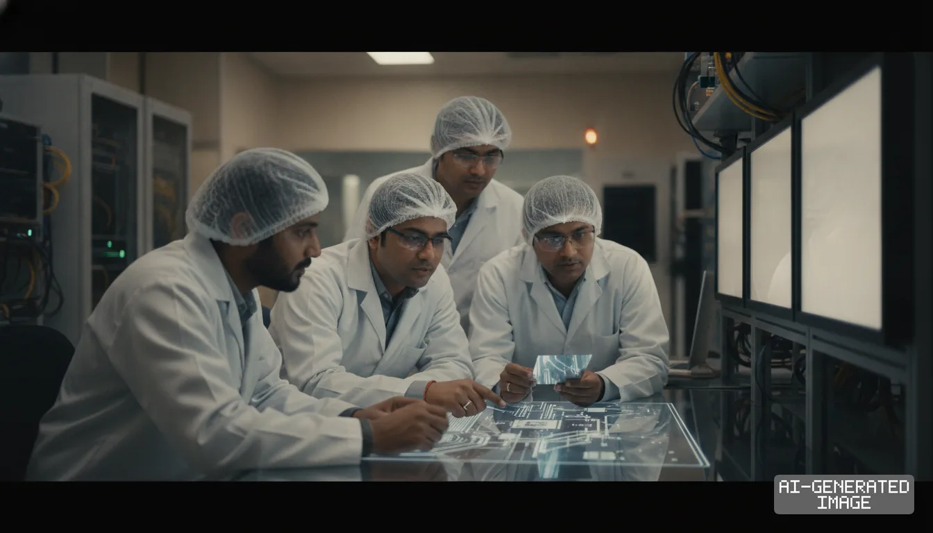
Rapidus and HCLTech opened two semiconductor engineering centers in India on Oct. 26, 2026, securing design support and software talent for Japan's planned 2-nanometer logic rollout.
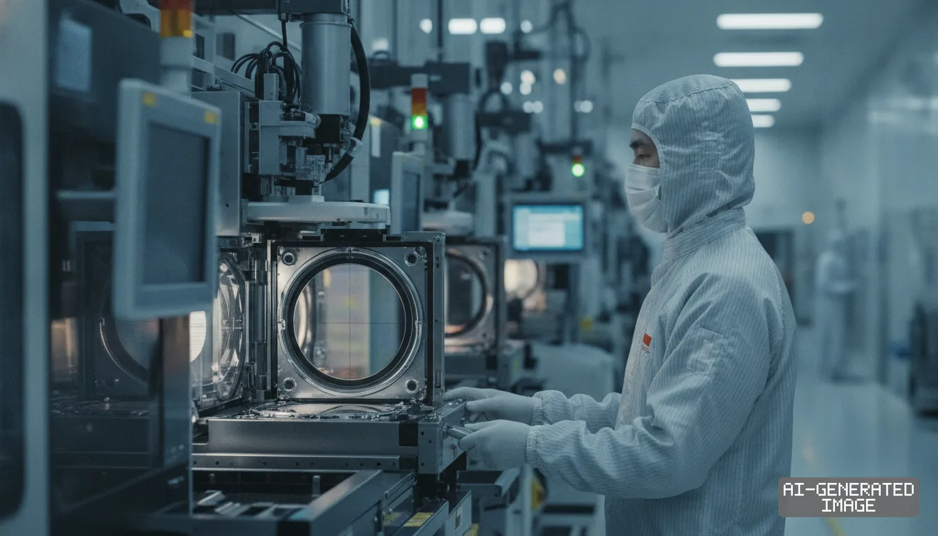
The dedicated facilities in Bengaluru and Hubli will handle chip design infrastructure, layout verification and process development. The sites support the Japanese foundry as it prepares its Hokkaido manufacturing plant for trial output.
HCLTech posted $14.8 billion in revenue for the 12 months ending September 2026. The Indian engineering firm deploys more than 2,000 silicon design engineers across global nodes ranging from 180nm to 2nm-class architectures.
Rapidus President and Chief Executive Officer Atsuyoshi Koike signed the agreement on Oct. 26, 2026, at HCLTech global headquarters in Noida, India. HCLTech Chief Executive Officer C Vijayakumar attended the signing ceremony.
The new centers will build process design kits—the standardized digital modeling files that chipless design houses require to align their circuits with a foundry's manufacturing line. Without mature kits, external customers cannot lay out transistors.
Engineers at the Karnataka sites will also carry out photomask design and layout engineering. Photomasks are quartz plates carrying circuit patterns that ultraviolet lithography equipment projects onto silicon wafers during fabrication.
The facilities will also run design technology co-optimization, an iterative engineering process where physical circuit design and chemical wafer processing are tuned together. The workflow improves transistor performance and cuts electrical leakage before tape-out.
HCLTech will also train and supply Indian semiconductor specialists to work at Rapidus facilities in Japan, the companies said. The recruitment channel addresses chronic engineering shortages across Japan's domestic microelectronics sector.
Japan lost its lead in advanced logic manufacturing after domestic conglomerates halted fab investment past the 45nm node two decades ago. The country retains equipment and chemical leadership but lacks deep pools of advanced digital designers.
Rapidus is building its initial wafer fabrication facility, dubbed Innovative Integration for Manufacturing, or IIM-1, in Chitose, Hokkaido. The venture aims to produce gate-all-around 2nm logic chips developed with research backing from IBM.
Foundries depend on third-party design houses to help fabless customers map custom circuits onto novel silicon nodes. A fab without third-party design enablement cannot attract high-volume commercial orders from artificial intelligence accelerator developers.
The Indian expansion builds directly on the Rapidus CORE ecosystem initiative unveiled on Oct. 5, 2026. That framework established external partnerships to accelerate production readiness across software, packaging, IP libraries and wafer fabrication.
As part of that framework, Rapidus launched its Design Solution Associates network with 17 partner companies. HCLTech was chosen as one of the 17 design providers tasked with delivering early-stage customer engineering support.
The Indian centers will support the foundry's proprietary manufacturing model, termed Rapid and Unified Manufacturing Service. The approach integrates front-end wafer fabrication directly with advanced packaging to reduce end-to-end design turnaround times.
Advanced packaging work will link with Rapidus Chiplet Solutions, a dedicated research cleanroom established within Seiko Epson's Chitose site in October 2024. The site develops pilot lines for silicon interposers and hybrid bonding.
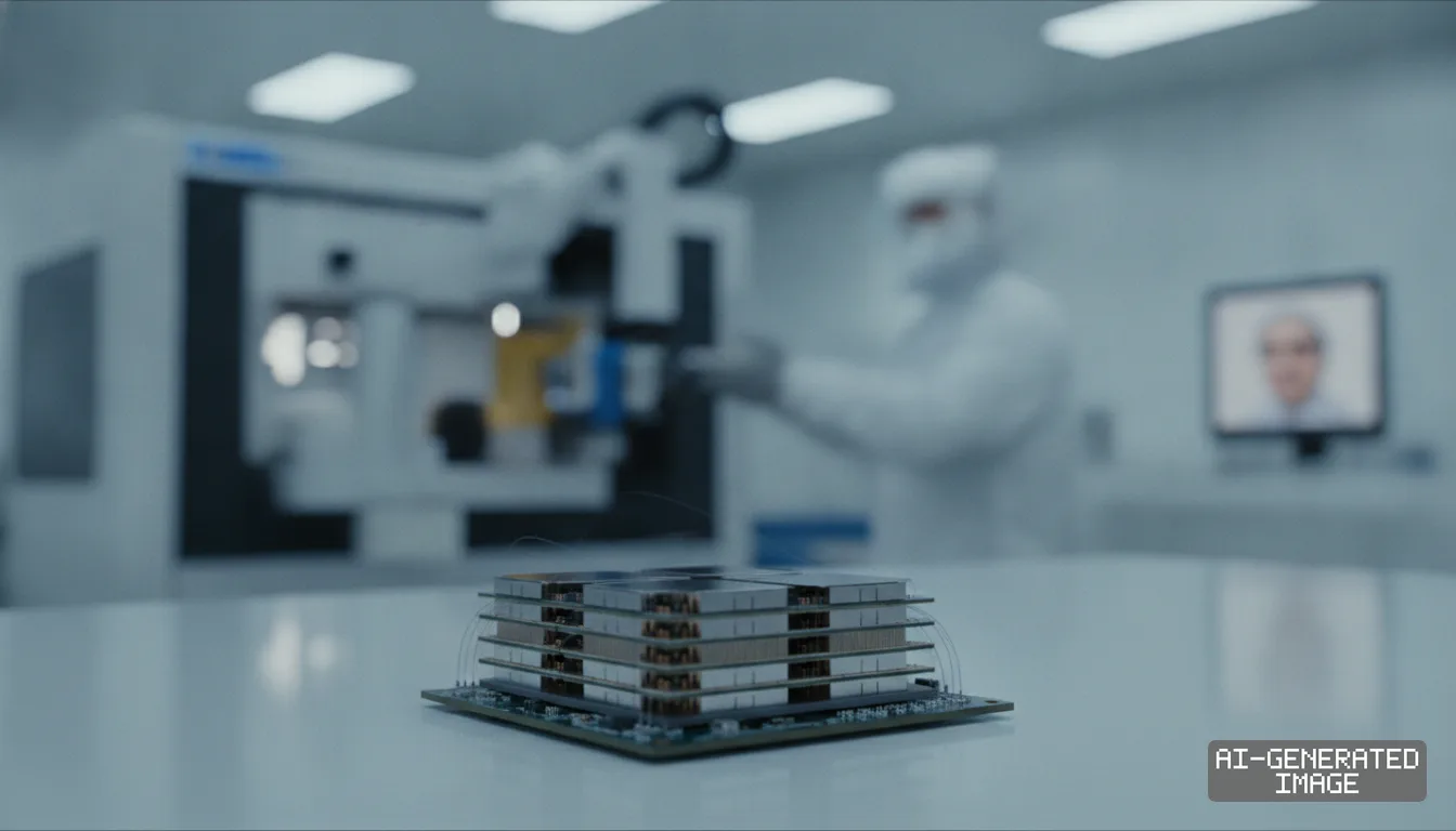
Modern artificial intelligence processors increasingly rely on chiplets—multiple smaller silicon dies mounted onto high-density substrates rather than a single monolithic chip. Designing these modules demands specialized thermal and electrical modeling.
HCLTech operates a 40,000-square-foot advanced semiconductor laboratory in Bengaluru with Class 1K and Class 10K cleanrooms. That facility performs post-silicon validation and automated test engineering, providing secondary hardware verification outside Japan.
The companies did not disclose the financial value of the contract or the specific engineering headcount assigned to the Bengaluru and Hubli centers. Rapidus has not published its total third-party service budget for fiscal 2026.
Rapidus plans to install extreme ultraviolet lithography systems and operate prototype pilot lines in Chitose through 2025, before targeting commercial 2nm volume production in 2027.
Impact map
How this development propagates across the region and out to global buyers.
| Event | Korea | China | Japan | Global impact |
|---|---|---|---|---|
| India 2nm engineering centers | no direct exposure, Samsung Electronics SF2 foundry monitors Japanese competition | no direct exposure, domestic fabs remain restricted below 7nm by multilateral controls | Rapidus narrows logic design deficit, securing Indian engineering pipeline for Chitose | fabless AI chip developers gain secondary 2nm design and tape-out route outside Taiwan |
In this story
- Companies
- Rapidus CorporationHCLTech
- Exposed
- IBMSeiko Epson
- Impact
- Supply ChainCost Structure
Related briefings
- Japan seeks $2.6B for Rapidus after pledging $21B to US fabs Also on IBM, Cost Structure
- Japan METI allocates clean power grid grants to anchor Hokkaido semiconductor hub Also on Rapidus Corporation, Cost Structure
- Rapidus forms 17-firm design alliance to back 2nm chip ramp Also on IBM
- Japan mask blank makers qualify High-NA EUV substrates for sub-2nm chips Also on Rapidus Corporation
Sources
Reporting
Confidence: medium — how we grade this
The documents behind this briefing are linked above. East Asia Brief produces its English text with AI assistance under human editorial review, and does not translate or republish other outlets' articles. See our methodology and AI policy. Spotted an error? Tell us.
The Morning Brief
What changed in Korean, Chinese and Japanese industry overnight — and what it means for your supply chain. One email, weekday mornings, US time. Free.
The Morning Brief is in preparation. Leave your address and we will write to you once — when the first issue is ready. Nothing before that.