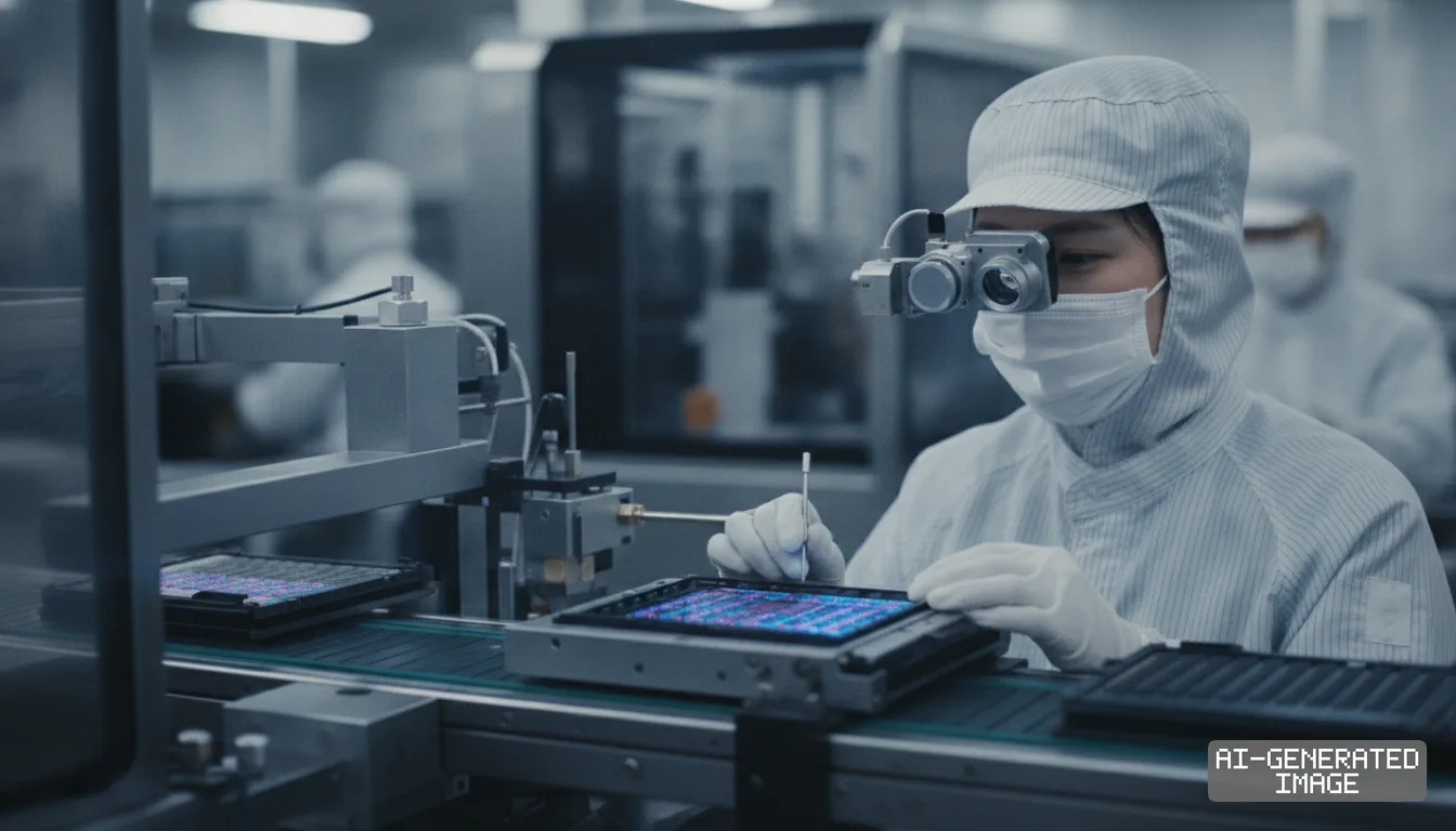
Apple deploys TSMC 2nm nanosheet silicon across A20 Pro processor dies
TechInsights teardown confirms a 98.2-square-millimeter compute die in the iPhone 18 Pro, marking the first commercial implementation of nanosheet transistors.
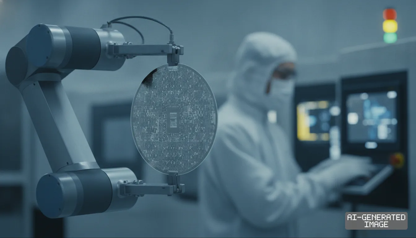
TechInsights released a reverse-engineering report Nov. 4, 2026, confirming that Apple's A20 Pro processor uses TSMC's two-nanometer gate-all-around nanosheet architecture across a 98.2-square-millimeter compute die.
The A20 Pro powers Apple's iPhone 18 Pro smartphone series released on Sept. 18. The handset line debuted following an official product unveiling at Apple's Cupertino headquarters on Sept. 9.
The compute die footprint of 98.2 square millimeters represents the first commercial implementation of nanosheet field-effect transistors in consumer hardware. Apple absorbed nearly all initial production volume from the foundry line.
Taiwan Semiconductor Manufacturing Company started volume production on its first-generation two-nanometer node, designated N2, during the fourth quarter of 2025. Fabrication takes place at TSMC's Fab 22 facility in Kaohsiung, Taiwan.
A gate-all-around transistor wraps conductive gates around stacked horizontal silicon nanosheets on all four sides. The physical geometry improves electrostatic channel control compared to older three-dimensional FinFET structures.
The nanosheet design cuts parasitic current leakage across the transistor channel during high-frequency operation. Power consumption drops by 25% to 30% at identical clock speeds, according to TSMC technical specifications.
Apple configured the central processing unit with two performance cores and four efficiency cores. The physical layout dedicates roughly 19% of logic floor space to the primary processing blocks.
A seven-core graphics engine and a dual 16-core neural processing unit occupy adjoining silicon territory. The integrated silicon provides dedicated hardware acceleration for on-device artificial intelligence workloads.
The teardown report confirmed that Apple abandoned traditional package-on-package stacking for system memory. Apple adopted TSMC's wafer-level multi-chip module packaging for the A3473 package assembly, the report said.
The packaging architecture places LPDDR5X mobile dynamic random-access memory horizontally beside the processor die. Earlier processor generations stacked memory packages directly on top of the logic silicon.
Horizontal memory placement shortens thermal dissipation paths through the handset vapor chamber cooling assembly. The layout prevents peak central processor heat from degrading memory retention speeds, the analysis said.
The physical die size of 98.2 square millimeters expanded by only 0.6% compared to the earlier three-nanometer A19 Pro. Aggressive logic cell scaling enabled Apple to add graphics and neural processing execution units without enlarging silicon dimensions.
Commercial quotes for TSMC's two-nanometer processed wafers exceed $30,000 per 300-millimeter disc. That price represents more than double the cost of mature five-nanometer foundry runs.
High wafer prices and tight capacity effectively blocked competing fabless designers from initial node allocations. Apple currently accounts for more than 20% of TSMC's consolidated annual foundry revenue.
Rival mobile processor designer Qualcomm opted to keep its flagship Snapdragon smartphone platforms on three-nanometer nodes. Qualcomm chose to avoid early pricing premiums on initial nanosheet capacity, supply chain filings show.
Taiwanese chip designer MediaTek similarly delayed its planned two-nanometer mobile processor tape-outs until mid-2027. MediaTek continues to manufacture its Dimensity flagship series on TSMC's enhanced three-nanometer lines.
The delay leaves Apple with an exclusive commercial performance window in high-end mobile silicon. Android handset manufacturers cannot access commercial two-nanometer application processors before the second half of 2027.
Samsung Electronics operates competing gate-all-around fabrication lines on its SF2 process in South Korea. The South Korean foundry failed to secure external tier-one mobile application processor contracts this year.
Samsung's logic fabrication division continues to face manufacturing yield hurdles for prospective external clients. The setback leaves TSMC with complete commercial pricing leverage in the sub-three-nanometer foundry market.
Surging silicon manufacturing costs are inflating bill-of-materials overhead for global premium smartphones. Foundry price hikes force device vendors to absorb thinner hardware operating margins on flagship tiers.
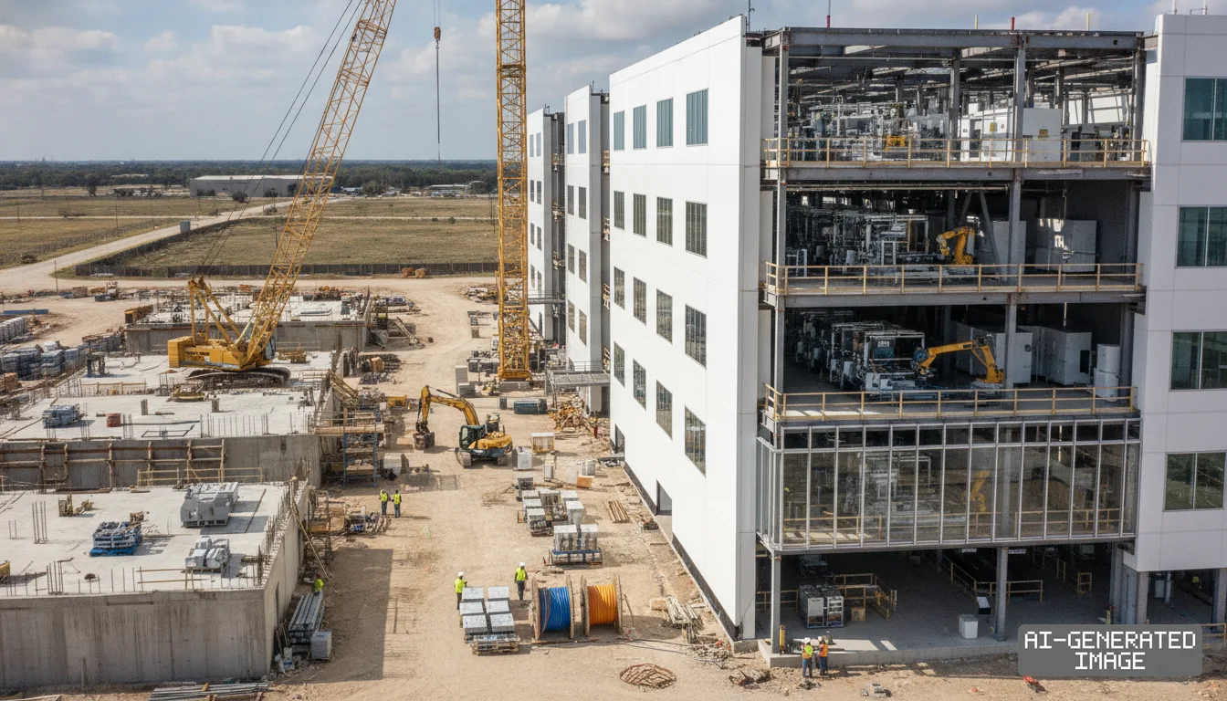
TSMC committed heavy capital expenditure to install advanced extreme ultraviolet lithography systems at Kaohsiung. The tooling requirements limit how quickly TSMC can build secondary fabrication lines for additional customers.
Fab 22 represents the first phase of an planned industrial complex spanning up to five fabrication phases in southern Taiwan. Capacity expansion remains tightly tied to committed long-term prepayments from top customers.
The companies have not published production yield rates for the N2 node, and operational defect densities are excluded from regulatory filings. TSMC and Apple classify precise wafer manufacturing yields as proprietary commercial trade secrets.
Industry estimates circulating among market analysts place commercial yield rates between 70% and 85%. Those speculative figures find no confirmation in audited financial disclosures or technical regulatory submissions.
TSMC schedules commercial production of its enhanced N2P manufacturing process in the second half of 2027. The revised node introduces backside power delivery rails to boost overall power distribution efficiency.
TSMC will report its full fourth-quarter 2026 financial metrics and capital spending allocations on Jan. 14, 2027.
Impact map
How this development propagates across the region and out to global buyers.
| Event | Korea | China | Japan | Global impact |
|---|---|---|---|---|
| TSMC 2nm commercialization | Samsung Electronics foundry misses flagship 2nm mobile AP contracts | MediaTek delays 2nm tape-outs to mid-2027 due to $30,000 wafer pricing | Tokyo Electron books deposition tool shipments for TSMC Fab 22 expansion | Apple controls initial 2nm capacity while rival smartphone platforms remain on 3nm |
In this story
- Companies
- AppleTSMC
- Tickers
- AAPL2330.TW
- Exposed
- QualcommMediaTekSamsung Electronics
- Impact
- Supply ChainCapexPricing
Related briefings
- Qualcomm keeps TSMC for 2nm processors, shutting out Samsung Foundry Also on MediaTek, Qualcomm, Apple
- TSMC raises 2nm wafer target to 120,000 units as orders surge Also on MediaTek, Qualcomm, Apple
- MediaTek debuts first 2nm mobile AP built on TSMC N2P node Also on MediaTek, Qualcomm, Apple
- Synopsys expands TSMC pact with agentic AI chip design tools for A14 Also on MediaTek
Sources
Primary documents
Reporting
Confidence: high — how we grade this
The documents behind this briefing are linked above. East Asia Brief produces its English text with AI assistance under human editorial review, and does not translate or republish other outlets' articles. See our methodology and AI policy. Spotted an error? Tell us.
The Morning Brief
What changed in Korean, Chinese and Japanese industry overnight — and what it means for your supply chain. One email, weekday mornings, US time. Free.
The Morning Brief is in preparation. Leave your address and we will write to you once — when the first issue is ready. Nothing before that.