Tokyo Ohka Kogyo opens 23 billion yen EUV photoresist plant
The Koriyama site expands domestic output of extreme ultraviolet lithography chemicals as the supplier controls over 35% of the global EUV resist segment.
Tokyo Ohka Kogyo prepared commercial production lines on Nov. 21, 2026 at its new 23 billion yen ($150 million) photoresist plant in Koriyama, expanding manufacturing capacity for advanced extreme ultraviolet lithography.
The Japanese chemical manufacturer supplies critical materials to advanced chipmakers worldwide. The company controls roughly 25% of the global semiconductor photoresist market and more than 35% of the extreme ultraviolet (EUV) photoresist segment.
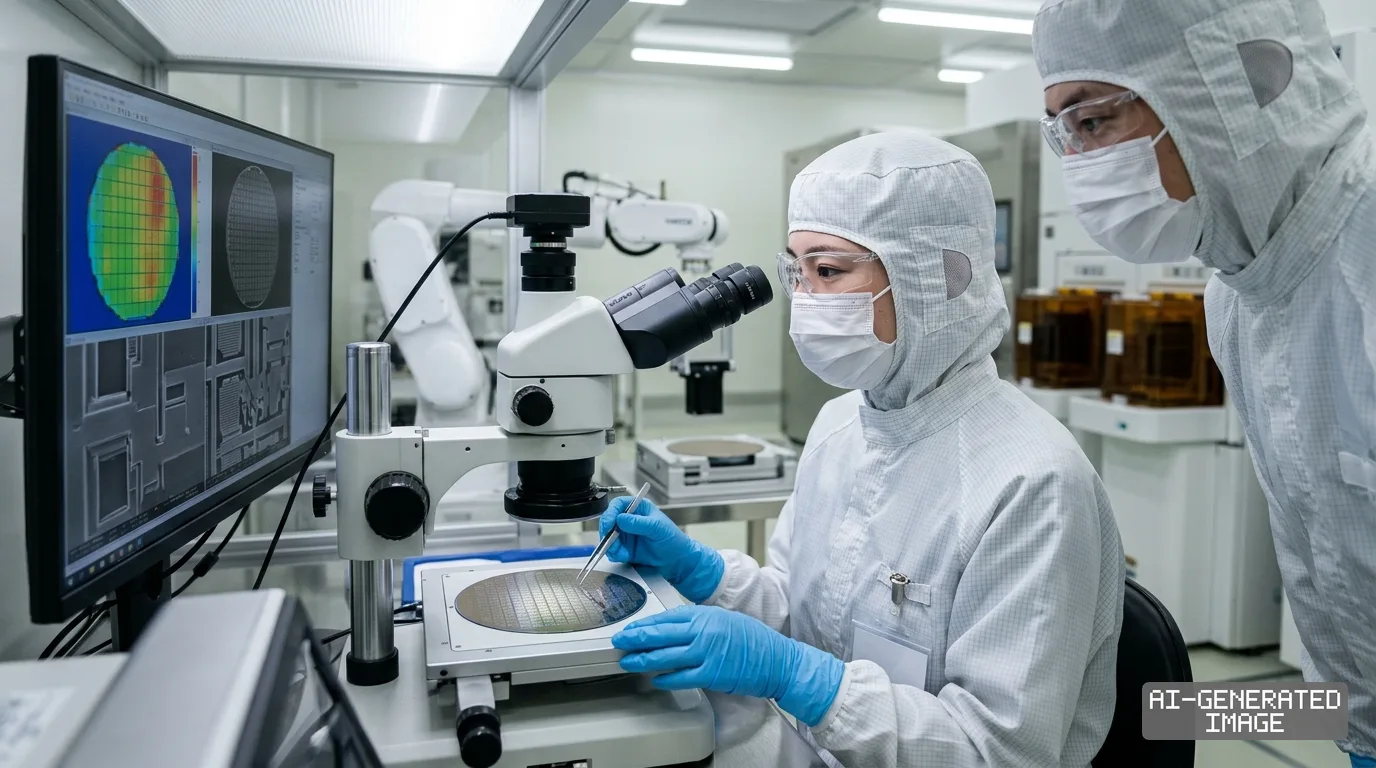
Extreme ultraviolet photoresists are light-sensitive chemical liquids applied to silicon wafers before exposure to laser light, enabling foundries to etch nanoscale circuit patterns. Advanced microchips require chemical formulations with high optical sensitivity to avoid structural defects.
The 23 billion yen capital expenditure represents the largest single facility investment in TOK's history. The capital outlay accounts for roughly 38% of the company's multi-year facility budget outlined in its corporate medium-term business plan.
The new manufacturing facility covers a building footprint of 4,800 square meters inside the existing Koriyama manufacturing complex in Fukushima Prefecture. TOK designates the site as the world's largest dedicated manufacturing building for semiconductor photoresists.
TOK broke ground on the Koriyama manufacturing building in July 2024 following board authorization in August 2023. Construction teams completed the building on Oct. 8, initiating cleanroom calibration and automated production line trials.
Taiwan Semiconductor Manufacturing Co. (TSMC) represents a primary consumer of TOK's lithography chemical output. TSMC accounts for an estimated 15% of TOK's electronic materials revenue, using advanced photoresists across sub-3-nanometer logic production lines.
Samsung Electronics relies on TOK formulations for memory chip production and contract manufacturing. Samsung deploys EUV lithography on dynamic random-access memory (DRAM) lines below the 14-nanometer node, where trace chemical purity directly dictates wafer yields.
TOK expanded testing facilities in South Korea to support regional chipmakers directly. The supplier completed a 7 billion yen ($46 million) inspection wing in Incheon and began building a 12 billion yen ($78 million) chemical plant in Pyeongtaek.
In Japan, TOK completed a high-purity chemical manufacturing facility at its Aso plant in Kumamoto Prefecture. That operation supplies critical processing solvents to Japan Advanced Semiconductor Manufacturing, the TSMC-majority foundry joint venture operating nearby.
Dutch toolmaker ASML Holding manufactures the scanner hardware that interacts directly with TOK's chemical coatings. ASML produces high-numerical-aperture EUV scanners priced at roughly $380 million each, systems requiring advanced photoresists engineered to prevent pattern collapse.
Higher numerical aperture lithography narrows optical depth of focus, forcing semiconductor fabricators to use thinner chemical resist films. Thinner coatings must absorb extreme ultraviolet photons more efficiently to maintain chemical contrast during plasma etching processes.
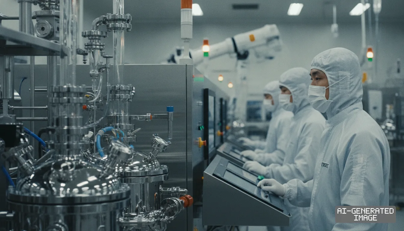
The Koriyama facility deploys automated mixing equipment and digital pipeline monitoring, the company said in an operational disclosure. Robotic handling minimizes human cleanroom presence, cutting airborne particulate contamination in bottles filled for advanced chip fabrication facilities.
Japanese suppliers dominate the international lithography materials sector, holding more than 80% of global semiconductor photoresist capacity. TOK competes against domestic peers including JSR, Shin-Etsu Chemical and Sumitomo Chemical to secure long-term purchase agreements with foundries.
Capital expenditure costs for the Koriyama site will not alter current annual financial guidance, the company said in an exchange filing. TOK incorporated project depreciation into consolidated earnings projections released on Aug. 6.
Strong demand for artificial intelligence server hardware lifted operational performance across lithography product lines. On Nov. 10, TOK raised its consolidated net sales forecast to 300 billion yen ($1.96 billion) and operating income projections to 63.5 billion yen.
The Koriyama expansion supports goals established under the corporate tok Medium-Term Plan 2027, which prioritizes supply chain security. The manufacturing site adds geographic redundancy, protecting material distribution against regional supply shocks and seismic disruptions in northeastern Japan.
Commercial operations and initial product shipments from the Koriyama facility begin before the end of November 2026, marking the operational handover of the completed manufacturing lines.
Tokyo Stock Exchange filings and company disclosures confirm no new capital expenditure decision was published on Nov. 21, 2026, and Tokyo Ohka Kogyo has not published separate annual output capacity figures for the Koriyama site.
Impact map
How this development propagates across the region and out to global buyers.
| Event | Korea | China | Japan | Global impact |
|---|---|---|---|---|
| Koriyama EUV photoresist plant | Samsung Electronics secures expanded certified resist options as Incheon testing site scales | Advanced foundries face continuous access restrictions for Japanese EUV resist supply | TOK expands domestic advanced materials base alongside Kumamoto chemical site | Advanced chipmakers secure dedicated High-NA EUV resist capacity across sub-3nm nodes |
In this story
- Companies
- Tokyo Ohka Kogyo
- Tickers
- 4186.T
- Exposed
- TSMCSamsung ElectronicsASML HoldingJSRShin-Etsu Chemical
- Impact
- Supply ChainCapexOrder Book
Related briefings
- Dongjin Semichem operating profit jumps 51% on photoresist surge Also on JSR, Tokyo Ohka Kogyo, Shin-Etsu Chemical
- Japan keeps South Korea on Group A strategic trade whitelist Also on JSR, Tokyo Ohka Kogyo, Shin-Etsu Chemical
- Mitsui Chemicals buys chip materials maker JSR for $11.6 billion Also on JSR, Tokyo Ohka Kogyo, Samsung Electronics
- SK hynix Convenes Japan Chip Suppliers on Next HBM Roadmap Also on JSR, Shin-Etsu Chemical
Sources
Reporting
Confidence: medium — how we grade this
The documents behind this briefing are linked above. East Asia Brief produces its English text with AI assistance under human editorial review, and does not translate or republish other outlets' articles. See our methodology and AI policy. Spotted an error? Tell us.
The Morning Brief
What changed in Korean, Chinese and Japanese industry overnight — and what it means for your supply chain. One email, weekday mornings, US time. Free.
The Morning Brief is in preparation. Leave your address and we will write to you once — when the first issue is ready. Nothing before that.