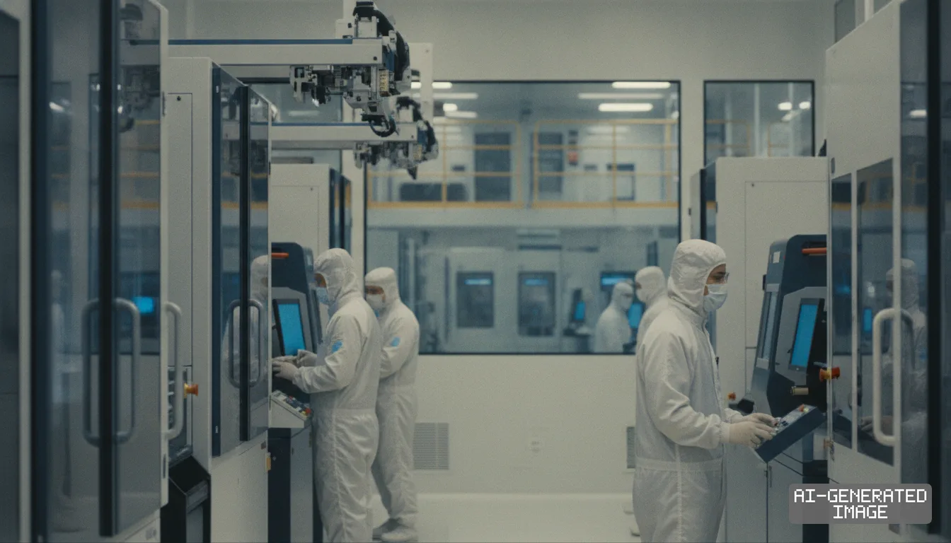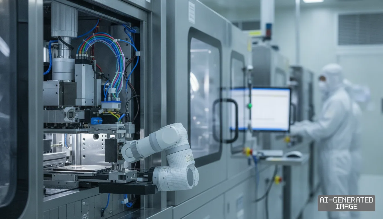
Samsung taps TSMC 3nm foundry to produce Nvidia NVHBM dies
The agreement shifts the Korean chipmaker away from an all-in-house turnkey manufacturing model after Nvidia mandated standard foundry sourcing across its custom memory suppliers.
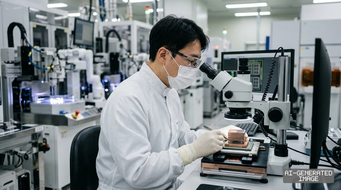
Samsung Electronics decided Oct. 18, 2026, to produce custom high-bandwidth memory base dies for Nvidia on Taiwan Semiconductor Manufacturing Co.’s 3-nanometer foundry node, shifting away from its proprietary turnkey packaging model.
The manufacturing shift allows Samsung to supply base dies for Nvidia’s custom NVHBM architecture. The architecture delivers up to 30% greater memory bandwidth and 15% lower power consumption than standard HBM4E memory stacks.
Taiwan Semiconductor Manufacturing Co., known as TSMC, controls roughly 62% of global dedicated foundry revenue. The contract chipmaker already manufactures Nvidia’s flagship artificial intelligence processors on advanced lithography lines in Taiwan.
Nvidia asked memory suppliers to unify manufacturing on TSMC’s 3-nanometer process for base dies. The base die sits beneath stacked dynamic random-access memory chips and routes electrical signals directly to the host graphics processing unit.
The architecture relocates the memory controller from the host compute die onto the base die. That design frees up to 25% more silicon area on Nvidia’s processors and reduces interface physical area by 67%.
Samsung will pair TSMC-fabricated logic base dies with its sixth-generation 10-nanometer class dynamic random-access memory. Industry engineers refer to this sixth-generation memory technology as 1c DRAM.
The decision marks Samsung’s first departure from an integrated turnkey strategy. The company historically built memory core dies, logic base dies and packaging lines entirely within its internal Device Solutions division.
Samsung previously showcased full internal capability on Feb. 12, 2026. The company announced mass production of sixth-generation HBM4 combining internal 1c DRAM with internal 4-nanometer base dies operating at 11.7 to 13 gigabits per second.
Nvidia required standardized base dies to eliminate duplicate quality verification procedures. Verifying separate base die architectures from multiple memory vendors creates substantial engineering overhead and slows platform qualification.
Micron Technology confirmed a matching outsourcing arrangement on Sept. 30, 2026. Micron executives told analysts during an earnings call that custom NVHBM base dies co-developed with Nvidia rely on TSMC advanced foundry nodes.
Micron posted $54.23 billion in revenue for its fourth fiscal quarter ending Sept. 3, 2026. Data center products accounted for roughly $18.00 billion of that quarterly total, up from $11.52 billion in the prior period.
SK hynix also agreed to use TSMC’s advanced foundry lines for next-generation base dies. SK hynix supplies more than 50% of Nvidia’s current high-bandwidth memory volume for artificial intelligence data centers.
The convergence on TSMC creates severe allocation pressure on advanced foundry lines. TSMC’s 3-nanometer manufacturing lines already run near full capacity to supply mobile processors and central processing units for major international technology clients.
Samsung maintains internal evaluations of its own 4-nanometer and sub-4-nanometer foundry capacity. The internal lines serve as a backup channel if TSMC cannot allocate sufficient wafer starts for NVHBM production volumes.
A dual-track approach protects Samsung against capacity bottlenecks at rival fabrication plants. The company intends to offer internal foundry base dies for standard JEDEC-compliant HBM4 products and non-Nvidia cloud customers.
Memory makers historically competed on DRAM cell density and stacking yields. Custom artificial intelligence architectures have forced memory vendors to behave like advanced logic subcontractors that handle intricate custom circuit designs.
The transition alters capital allocation across the semiconductor industry. Memory producers must absorb external foundry processing fees, while pure-play foundries capture revenue previously retained by vertically integrated device manufacturers.
External foundry wafer processing costs for 3-nanometer silicon exceed $20,000 per wafer. Custom packaging margins remain high enough to offset those procurement costs because custom memory commands substantial price premiums over commodity DRAM.
Packaging integration also requires tight technical coordination with specialized packaging houses. Interposers and high-density substrate connections require microscopic interconnect pitches that standard printed circuit board assembly facilities cannot support.
South Korea’s semiconductor equipment supply chain faces indirect realignments from the shift. Domestic tool vendors developed deposition and etching tools optimized for Samsung’s proprietary packaging lines rather than TSMC’s wafer fabrication standards.
TSMC’s ecosystem partners in Taiwan stand to gain supplementary processing contracts. Taiwanese testing facilities and intermediate substrate suppliers handle high volumes of TSMC’s advanced packaging output under its CoWoS manufacturing framework.
Nvidia plans to deploy the custom NVHBM architecture in next-generation accelerator hardware. Platform verification trials for initial silicon samples are scheduled to begin across server original equipment manufacturers in mid-2027.
The companies have not published a tripartite supply agreement, and public filings do not disclose the precise volume split between TSMC and Samsung’s internal foundry lines.
Market participants await formal commercial terms during corporate reporting cycles. Samsung reports third-quarter financial results on Oct. 31, 2026, when executives will address foundry capital spending and custom memory shipment timelines.
Sources
Reporting
The documents behind this briefing are linked above. East Asia Brief produces its English text with AI assistance under human editorial review, and does not translate or republish other outlets' articles. See our methodology and AI policy. Spotted an error? Tell us.
The Morning Brief
What changed in Korean, Chinese and Japanese industry overnight — and what it means for your supply chain. One email, weekday mornings, US time. Free.
The Morning Brief is in preparation. Leave your address and we will write to you once — when the first issue is ready. Nothing before that.