Rapidus adopts multi-fab cluster model for Hokkaido 2nm logic site
Japan's METI approved 631.5 billion yen in fiscal 2026 cleanroom subsidies to back the venture's 5 trillion yen roadmap.
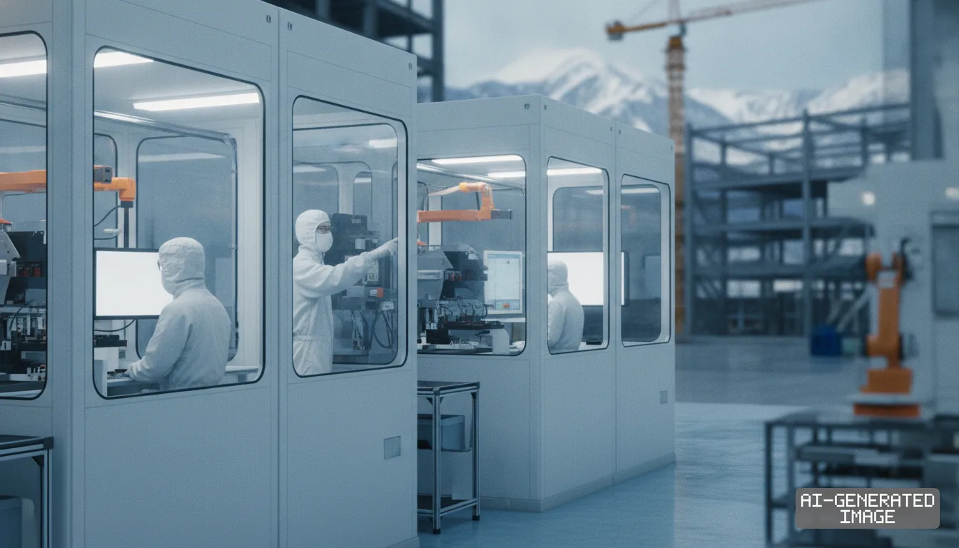
Rapidus moved to structure its Hokkaido manufacturing site around a multi-fab cluster model on Nov. 10, 2026, as the Japanese venture aligns its 2-nanometer foundry schedule with regional suppliers.
The venture operates within a 5 trillion yen ($33 billion) total capital roadmap. The Ministry of Economy, Trade and Industry approved 631.5 billion yen ($4.1 billion) in fiscal 2026 subsidies to fund cleanroom equipment and trial production runs.
The approved subsidy represents roughly 80% of state semiconductor support allocated under METI's Post-5G project this fiscal year. Rapidus also secured 267.6 billion yen in equity earlier in 2026, including 100 billion yen from the state-backed Information-technology Promotion Agency.
The foundry model mirrors Taiwan's Hsinchu Science Park, where silicon fabrication lines operate alongside testing laboratories, chemical suppliers and substrate packaging facilities. Rapidus aims to replicate that spatial density across its Chitose industrial footprint.
Construction of the venture's first facility, Innovative Integration for Manufacturing-1, reached operational readiness for tool installation in Chitose. Engineers at the facility began electrical testing on 2-nanometer gate-all-around transistor structures after connecting automated material handling systems.
The broader Chitose site design reserves parcels for up to three additional fabrication buildings, designated IIM-2, IIM-3 and IIM-4. The planned expansions would accommodate sub-2-nanometer nodes as production lines scale beyond initial trial volumes.
Rapidus and the Ministry of Economy, Trade and Industry have not published official site filings or construction schedules for the proposed IIM-2, IIM-3 and IIM-4 fabrication lines. The venture has not committed capital to secondary ground preparation.
Land development near the Chitose fab expanded through a municipal agreement signed on Oct. 23. Mitsubishi Estate, Chitose City and NTT Docomo Business partnered to establish an industrial research hub called Chitose Technology Frontier.
The development covers 129,000 square meters inside the Chitose Bibi World industrial zone. Mitsubishi Estate manages physical area planning, while NTT Docomo Business installs high-capacity fiber communications networks to link incoming laboratory tenants.
The consortium targets the first operational phase of the research park in fiscal 2029. The site is structured to house university laboratories, equipment maintenance engineers and specialized materials testing facilities directly adjoining the foundry boundary.
Commercial infrastructure around the foundry gained complementary office facilities this year. Mitsui Fudosan opened a dedicated enterprise hub at New Chitose Airport, providing flexible workspaces for suppliers and engineering teams traveling between Tokyo and Hokkaido.
Advanced packaging forms a central component of the Chitose cluster strategy. Rapidus opened its Analysis Center and Rapidus Chiplet Solutions facility on April 11, placing back-end processing directly adjacent to the front-end wafer fab.
Separating front-end lithography from back-end packaging across distant prefectures creates logistics bottlenecks, the venture said. Co-locating chiplet assembly in Chitose allows engineers to cut turnaround times for complex artificial intelligence silicon.
METI allocated 117.4 billion yen of its fiscal 2026 Rapidus budget specifically to packaging research and development. The remaining 514.1 billion yen supports front-end transistor fabrication, lithography trials and single-wafer processing systems.
Private Japanese corporations committed 167.6 billion yen to the venture across 32 corporate backers. Toyota Motor, Nippon Telegraph and Telephone and SoftBank Group hold equity stakes, seeking domestic supply security for automotive and artificial intelligence silicon.
Equipment manufacturers have also established local field offices in Chitose to support lithography systems. ASML Holding delivered its Twinscan NXE:3800E extreme ultraviolet scanner to New Chitose Airport, marking the first commercial EUV installation in Japan.
Rapidus plans to install up to 10 extreme ultraviolet lithography machines across its first two manufacturing facilities, company leadership said. Each high-precision scanner requires dedicated vendor engineering teams for optics alignment and vacuum maintenance.
Customer design access expanded through the launch of the Rapidus CORE alliance on Oct. 5. The partnership enrolled 17 design solution associates, including Cadence Design Systems, Synopsys and Toppan, to support customer layout preparation.
The venture developed a preliminary Process Design Kit for advance evaluation by prospective fabless clients. Rapidus aims to distribute the finalized kit to customers by early 2026, allowing design teams to configure prototype tape-outs.
Initial foundry capacity focuses on customized logic for artificial intelligence data centers. Demand for 2-nanometer wafers could outstrip global supply by 10% to 30% by 2030, according to METI implementation projections.
International technical cooperation underpins the Chitose manufacturing process. Rapidus developed its gate-all-around architecture through joint research with IBM at the Albany NanoTech Complex in New York, alongside semiconductor consortium imec in Belgium.
The venture also expanded European technical ties in June, signing memorandums of understanding with the UK Semiconductor Centre and Italy's Chips-IT foundation. The agreements aim to develop joint research programs and European customer relationships.
Chitose offers distinct environmental conditions for high-volume chip manufacturing. The local Chitose River provides abundant fresh water required for wafer cleaning, while Hokkaido maintains extensive renewable energy generation capacity.
Engineering recruitment has matched cleanroom preparation. Rapidus expanded its full-time workforce past 1,200 staff, transferring semiconductor specialists from across Japan while training technical graduates for Chitose cleanroom operations.
Commercial production schedules remain pegged to firm deadlines. Rapidus targets full mass production at IIM-1 in the second half of fiscal 2027, followed by a planned public listing around fiscal 2031.
The venture expects to report operating cash-flow breakeven around fiscal 2029 as production lines reach commercial volume manufacturing in Hokkaido, according to METI filings.
Impact map
How this development propagates across the region and out to global buyers.
| Event | Korea | China | Japan | Global impact |
|---|---|---|---|---|
| Chitose semiconductor cluster expansion | Samsung foundry faces alternative 2nm manufacturing base outside Taiwan | tightened domestic supply chain buffers regional logic demand against export rules | Chitose anchors domestic 2nm fabrication backed by 631.5 billion yen in subsidies | fabless AI chip developers gain non-Taiwan advanced packaging and foundry capacity |
In this story
- Companies
- Rapidus
- Exposed
- Mitsubishi EstateNTT DocomoASML HoldingToyota Motor
- Policy
- Subsidies
- Impact
- CapexSupply Chain
Track every Subsidies development →
Related briefings
- Japan seeks $2.6B for Rapidus after pledging $21B to US fabs Also on Rapidus, Toyota Motor, Subsidies
- Rapidus forms 17-firm design alliance to back 2nm chip ramp Also on Rapidus, Toyota Motor, Subsidies
- SMIC hits record $9.33B revenue as legacy nodes mask 7nm lag Also on ASML Holding, Subsidies
- Elon Musk rejects TSMC Terafab deal, backing Intel 14A node Also on ASML Holding, Subsidies
Sources
Primary documents
Reporting
Confidence: high — how we grade this
The documents behind this briefing are linked above. East Asia Brief produces its English text with AI assistance under human editorial review, and does not translate or republish other outlets' articles. See our methodology and AI policy. Spotted an error? Tell us.
The Morning Brief
What changed in Korean, Chinese and Japanese industry overnight — and what it means for your supply chain. One email, weekday mornings, US time. Free.
The Morning Brief is in preparation. Leave your address and we will write to you once — when the first issue is ready. Nothing before that.