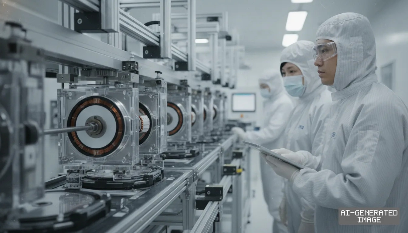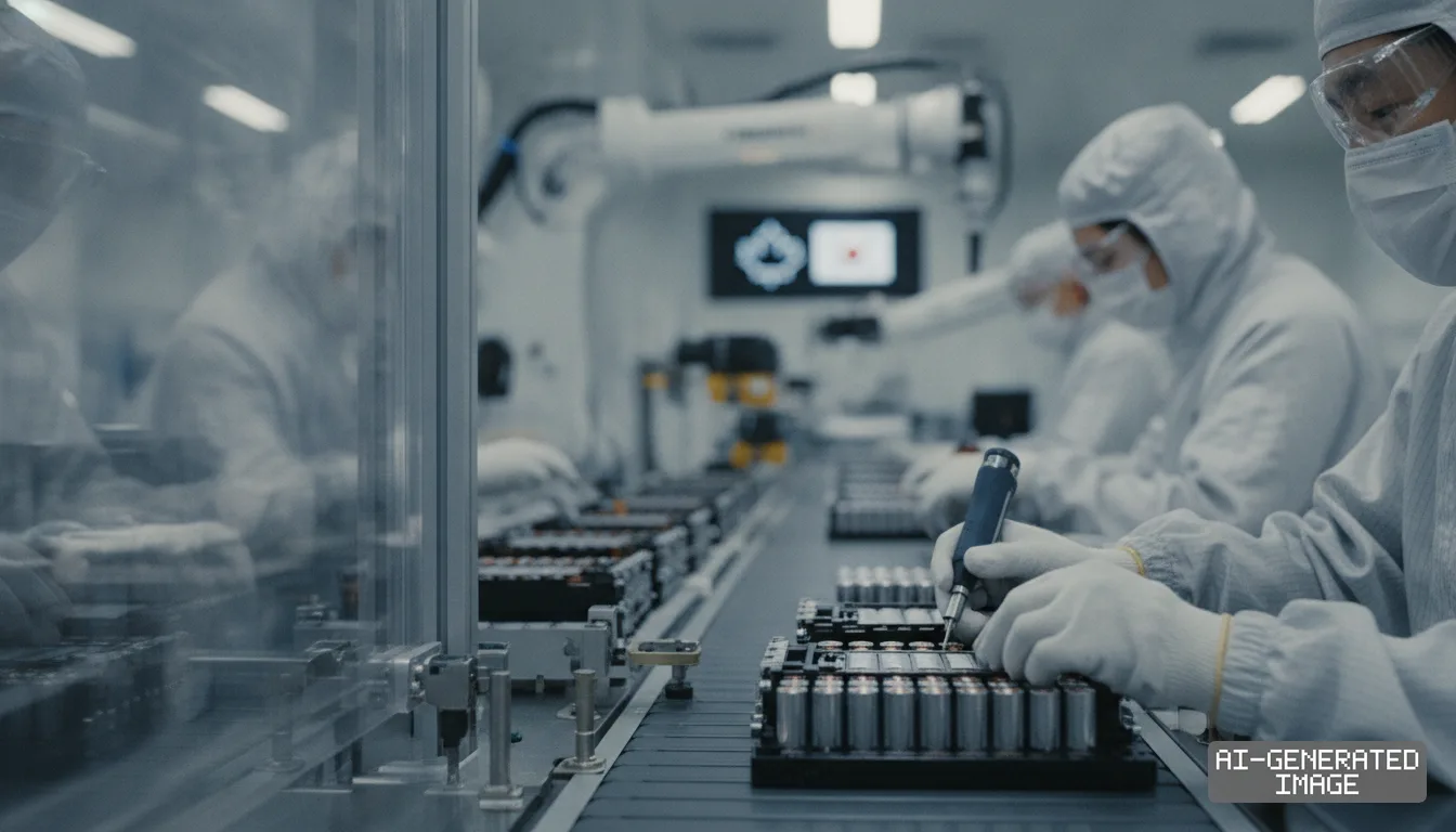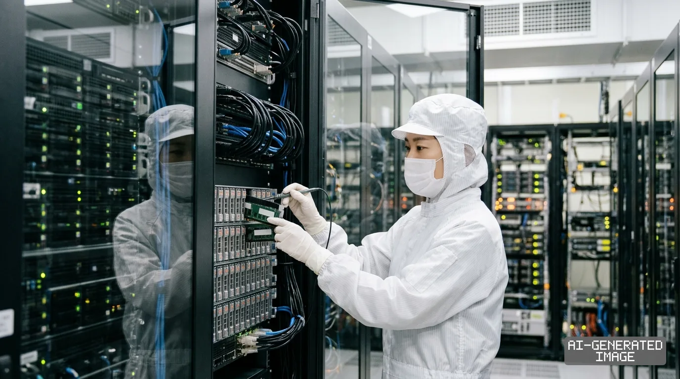
TSMC and Samsung freeze sub-16nm chip shipments to Chinese clients
The contract manufacturers paused wafer lines below 16 nanometers to review blueprints under tighter US controls, affecting markets that generate 11% of TSMC revenue.
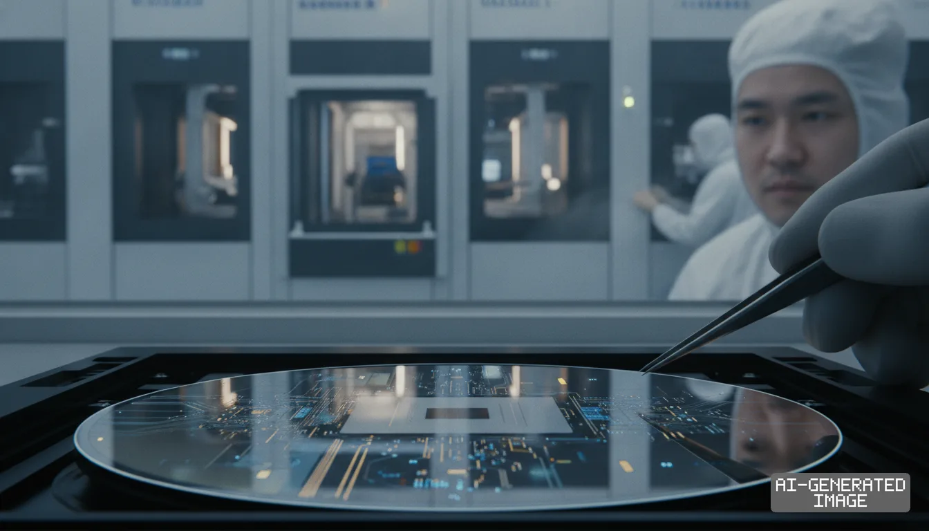
Taiwan Semiconductor Manufacturing Co. and Samsung Electronics suspended shipments of select advanced chips to Chinese design firms on Nov. 19, 2026, after the United States government expanded export controls.
The measure halts wafer processing at nodes below 16 nanometers while both foundries review customer blueprints against revised compliance thresholds. Neither contract manufacturer can deliver finished silicon without an approved export permit from Washington.
Mainland China generated 11% of TSMC's consolidated revenue in the third quarter of 2026, equal to about $2.6 billion. For Samsung Electronics, Chinese clients account for an estimated 12% of external foundry orders across advanced and mature fabrication lines.
The United States Bureau of Industry and Security published an interim final rule on Nov. 15, 2026, taking legal effect in the Federal Register on Nov. 19, 2026. The regulation restricts remote access to advanced computing infrastructure.
The updated framework also closes packaging channels that permitted Chinese designers to ship unfinished wafers to third-party assembly contractors. Those outside packaging houses previously assembled multichip modules without submitting designs to the primary foundry for compliance review.
Under the new provisions, foundries must verify downstream assembly configurations before beginning wafer fabrication. If a customer uses an unverified packaging facility, the foundry must secure an export license directly from the Department of Commerce.
The directive builds upon comprehensive export curbs introduced on Oct. 7, 2022, and updated in October 2023. Commerce Department officials previously sent an administrative notice to TSMC on Nov. 11, 2024, halting 7-nanometer GPU shipments to Chinese clients.
The latest revision extends scrutiny beyond artificial intelligence accelerators to general-purpose computing processors and advanced smartphone silicon. That broader scope directly affects major Chinese internet platforms and consumer device manufacturers.
Baidu's chip design subsidiary Kunlun relies on external foundries for 100% of its second-generation and third-generation AI accelerators. ByteDance contracts out manufacturing for its internal recommendation chips, processing tens of thousands of wafers annually.
Smartphone makers Xiaomi, Oppo and Vivo also face supply disruption. All three companies use external foundries to produce proprietary image signal processors and neural processing units fabricated at 12-nanometer and smaller process nodes.
Foundries must now hold unfinished silicon in cleanroom storage while export license applications undergo interagency review in Washington. Historical review cycles for advanced computing licenses have typically taken between four and nine months to conclude.
TSMC operated its 7-nanometer and 5-nanometer lines at roughly 88% capacity utilization during the third quarter. Samsung Electronics operates its contract fabrication unit below 70% utilization, relying on Chinese design houses to fill available production lines in Pyeongtaek.
Chinese fabless designers cannot easily replace foreign foundries with domestic suppliers. Semiconductor Manufacturing International Corp., China's largest contract chipmaker, faces equipment constraints that restrict its sub-14-nanometer capacity to roughly 20,000 wafer starts per month.
Commercial device makers face multi-quarter redesign delays if forced to alter physical chip layouts for alternate foundries. Developing an advanced chiplet architecture requires 12 to 18 months and costs more than $50 million in engineering labor and design software.
The interim final rule establishes a 60-day public comment period that closes on Jan. 18, 2027. Commerce Department officials plan to evaluate industry feedback before issuing a finalized permanent regulation later in 2027.
Neither TSMC nor Samsung Electronics has published a regulatory filing detailing the exact wafer volumes or customer contracts frozen by the action. The Commerce Department notice also omits estimates of affected commercial revenue.
United States export control officers continue to audit foundry customer rosters across East Asia. Foundries that ship covered items without approved authorization face administrative penalties and loss of access to American electronic design tools and fabrication equipment.
Impact map
How this development propagates across the region and out to global buyers.
| Event | Korea | China | Japan | Global impact |
|---|---|---|---|---|
| Advanced foundry export rule | Samsung faces utilization risk on sub-7nm lines, where China provides ~12% of external orders | Baidu and ByteDance face 4-9 month licensing delays for custom AI accelerators | Tokyo Electron and Canon face deferred tool installations at Chinese packaging sites | AI server and mobile chip lead times extend 12-18 months on forced architecture redesigns |
In this story
- Companies
- Taiwan Semiconductor Manufacturing Co.Samsung Electronics
- Tickers
- 2330.TW005930.KS
- Exposed
- BaiduByteDanceXiaomi
- Policy
- Export Controls
- Impact
- Supply ChainOrder BookCompliance
Track every Export Controls development →
Related briefings
- CXMT beats SK hynix and Micron in DRAM margin at 87.59% gross rate Also on ByteDance, Xiaomi, Samsung Electronics
- China exempts overseas AI model APIs from draft export rules Also on Baidu, Export Controls, Compliance
- China curbs exports of 40 AI, solar and biotech technologies Also on Baidu, Export Controls, Compliance
- China Tightens Connected Vehicle Data Rules With Mandatory Local Sensor Scrubbing Also on Baidu, Export Controls, Compliance
Sources
Primary documents
Reporting
Confidence: high — how we grade this
The documents behind this briefing are linked above. East Asia Brief produces its English text with AI assistance under human editorial review, and does not translate or republish other outlets' articles. See our methodology and AI policy. Spotted an error? Tell us.
The Morning Brief
What changed in Korean, Chinese and Japanese industry overnight — and what it means for your supply chain. One email, weekday mornings, US time. Free.
The Morning Brief is in preparation. Leave your address and we will write to you once — when the first issue is ready. Nothing before that.