TSMC Accelerates AP7 and AP8 Fabs to Ease AI Packaging Crunch
Equipment lead times have stretched to eight months as the foundry targets monthly CoWoS output of 130,000 wafers this year and 200,000 in 2027 to feed Nvidia and AMD.
MOBy Mina Okoro, Supply chain editor··Updated October 29, 2026·4 min read
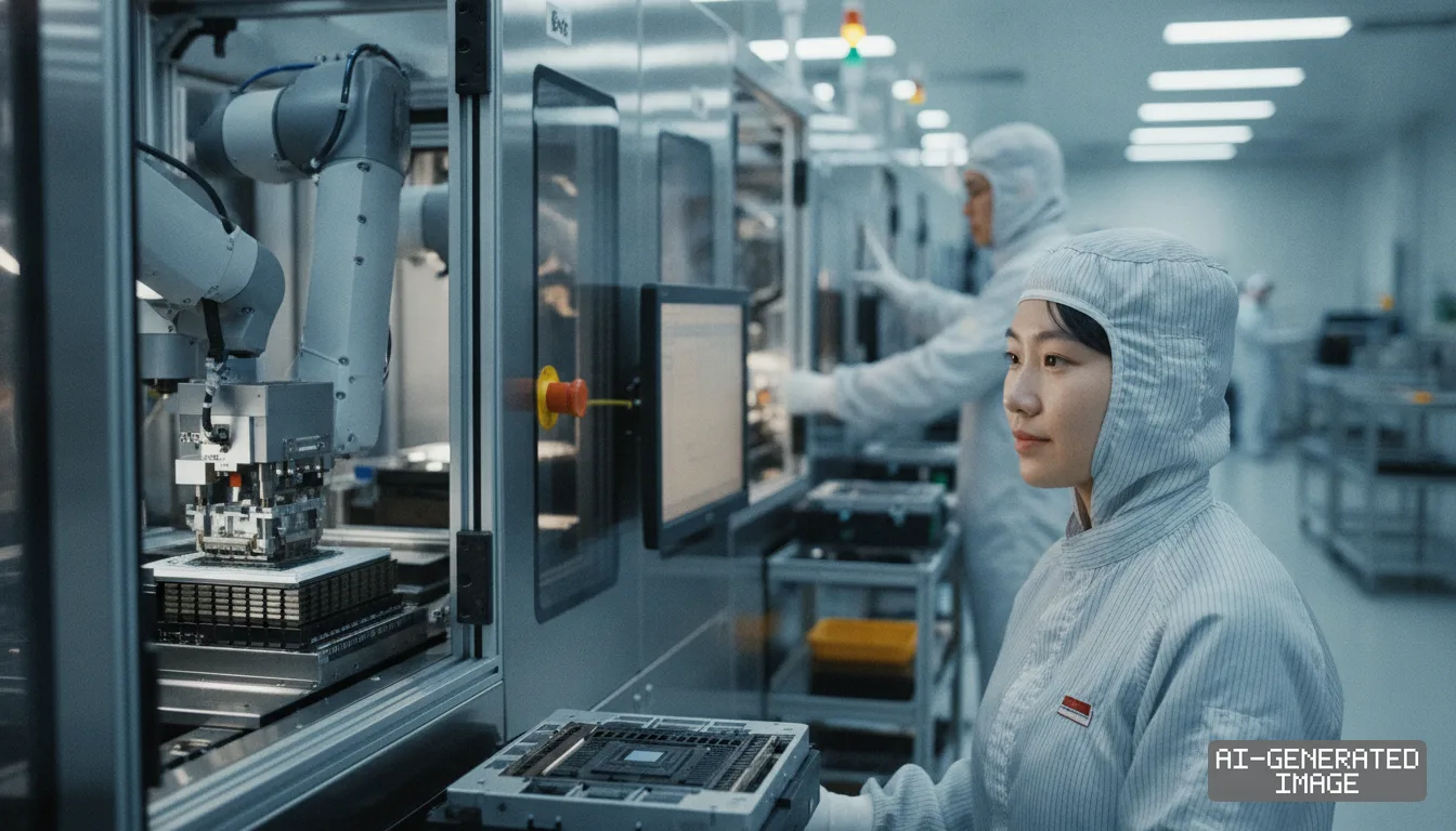
ShareLinkedInXWhatsAppEmailWorkers in cleanroom suits monitor automated robotic equipment handling semiconductor packaging inside a plant. (AI-generated image)
TSMC accelerated tool installations on Oct. 29, 2026 at its AP7 and AP8 advanced packaging plants in southern Taiwan, pushing to clear a chronic bottleneck in CoWoS capacity.
The expansion targets a packaging shortfall that restricts shipments of artificial intelligence accelerators. A finished logic wafer cannot ship until bonded with memory, making packaging rather than wafer fabrication the primary gating factor.
The documents behind this briefing are linked above. East Asia Brief produces its English text with AI assistance under human editorial review, and does not translate or republish other outlets' articles. See our methodology and AI policy. Spotted an error? Tell us.
Supply chain editor — Mina Okoro builds the impact maps that connect East Asian developments to buyers in North America and Europe, and edits the Asia Compare desk.