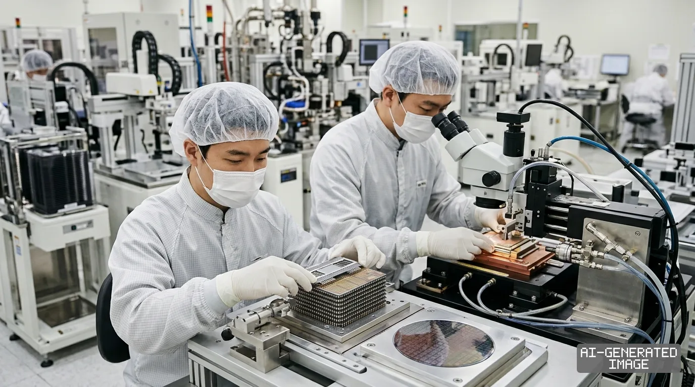
Nvidia expands Asian packaging network to break AI server bottlenecks
Multiyear supply pacts across South Korea, Japan and Taiwan will lift packaging substrate capacity 2.5 times and interposer volume 300% through 2028.
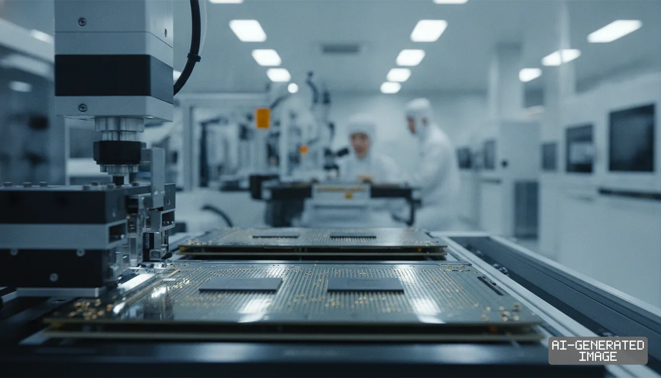
Nvidia announced multiyear manufacturing agreements on Oct. 21, 2026, to expand advanced packaging, substrate fabrication and testing capacity across Asia and the United States.
The transactions target a 2.5-fold increase in dedicated packaging substrate output over the next three years, representing the bulk of carrier board supply for next-generation computing hardware.
Chief executive Jensen Huang said at the GTC Berlin conference that extraordinary computing demand across hyperscale data centers requires immediate factory expansions to resolve severe packaging constraints.
The agreements distribute high-density multi-chip packaging operations away from single-site bottlenecks in Taiwan, establishing parallel manufacturing corridors across South Korea, Japan and the United States.
Under the plan, Amkor Technology agreed to increase its interposer wafer packaging capacity in South Korea by more than 300% by the end of 2028.
Amkor will construct and tool dedicated cleanroom bays in South Korea to process silicon interposers that bridge logic dies and high-bandwidth memory stacks, the company said.
The interposer expansion supports complex 2.5-dimensional module assemblies, which have limited total accelerator shipments throughout the current infrastructure investment cycle, according to supply chain disclosures.
Samsung Electro-Mechanics joined Nvidia's supplier roster under a multiyear contract to fabricate Ajinomoto build-up film package substrates, entering commercial deliveries before the close of 2026.
Samsung Electro-Mechanics will allocate existing domestic manufacturing lines and expand dedicated facilities across its Sejong and Busan campuses to produce high-density multi-layer boards.
Production allocated to Nvidia is scheduled to absorb a significant portion of Samsung Electro-Mechanics' total annual package substrate capacity by 2028, the component vendor said.
The South Korean supplier integrates thin-film capacitors and embedded passives within the core layers, aiming to reduce voltage droop across dense processor interconnects.
In Japan, Ibiden received a multibillion-dollar capacity reservation advance from Nvidia to fund a major expansion at its Ono manufacturing plant in Gifu Prefecture.
The capital commitment will triple high-end substrate manufacturing capacity at the Ono plant, with initial commercial production lines scheduled to ramp during the first quarter of 2028.
Ibiden remains the principal supplier of large-body packaging substrates for high-performance computing dies, but historical fabrication limits prompted Nvidia to finance dedicated production machinery directly.
Taiwanese substrate manufacturer Unimicron Technology signed a parallel capacity reservation agreement to expand manufacturing lines at its KF production site in Taoyuan.
Unimicron plans to commence commercial volume shipments from the expanded Taiwanese facility in the second quarter of 2027, reaching maximum rated throughput by mid-2028, the company said.
The addition of Unimicron and Samsung Electro-Mechanics creates a three-way substrate sourcing structure, reducing reliance on single-plant production schedules across East Asia.
Downstream testing infrastructure will also expand under a $1.1 billion capacity reservation advance paid to Taiwanese testing contractor King Yuan Electronics, known as KYEC.
KYEC will use the funds to establish specialized semiconductor testing facilities in the United States, supporting advanced multi-chip system qualification outside of its primary East Asian base.
The testing contract supports an anticipated doubling of Nvidia's total semiconductor testing capacity between calendar 2026 and 2027 across operational hubs in Taiwan, Singapore and North America.
KYEC plans to achieve high-volume commercial testing throughput at the new American facility in April 2027, according to contractual milestones established in the agreement.
For optical interconnects, Siliconware Precision Industries, or SPIL, agreed to scale manufacturing capacity for co-packaged optics engines by 15 times by mid-2027.
SPIL targets an additional doubling of optical engine output by the end of 2028, providing optical transceivers designed to bypass electrical board traces in hyperscale rack architectures.
The official notice does not state the specific dollar value of the advance payment to Ibiden, and Samsung Electro-Mechanics has not published the total capital expenditure allocated to its Sejong and Busan factories.
The scheduled calendar milestone requires KYEC to commence high-volume commercial testing runs in the United States in April 2027, preceding substrate ramps across Japan and South Korea in 2028.
Sources
Reporting
The documents behind this briefing are linked above. East Asia Brief produces its English text with AI assistance under human editorial review, and does not translate or republish other outlets' articles. See our methodology and AI policy. Spotted an error? Tell us.
The Morning Brief
What changed in Korean, Chinese and Japanese industry overnight — and what it means for your supply chain. One email, weekday mornings, US time. Free.
The Morning Brief is in preparation. Leave your address and we will write to you once — when the first issue is ready. Nothing before that.