IBM opens Chitose office to back Rapidus on 2nm chip line
The base brings IBM software and transistor engineers beside Rapidus as Japan backs its 2-nanometer foundry with 2.35 trillion yen in research aid.
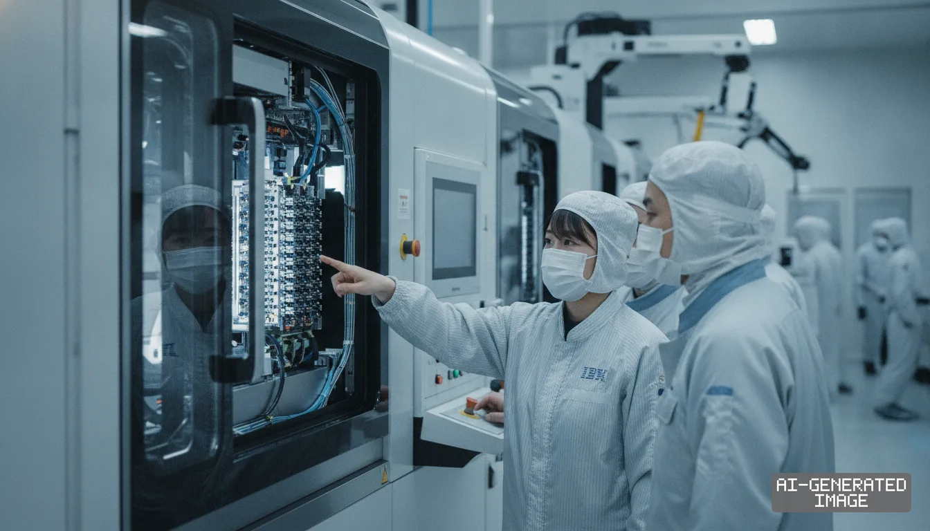
IBM opened a technical base in Chitose, Japan on Oct. 27, 2026, deploying engineers beside foundry startup Rapidus to accelerate pilot testing of 2-nanometer logic chips.
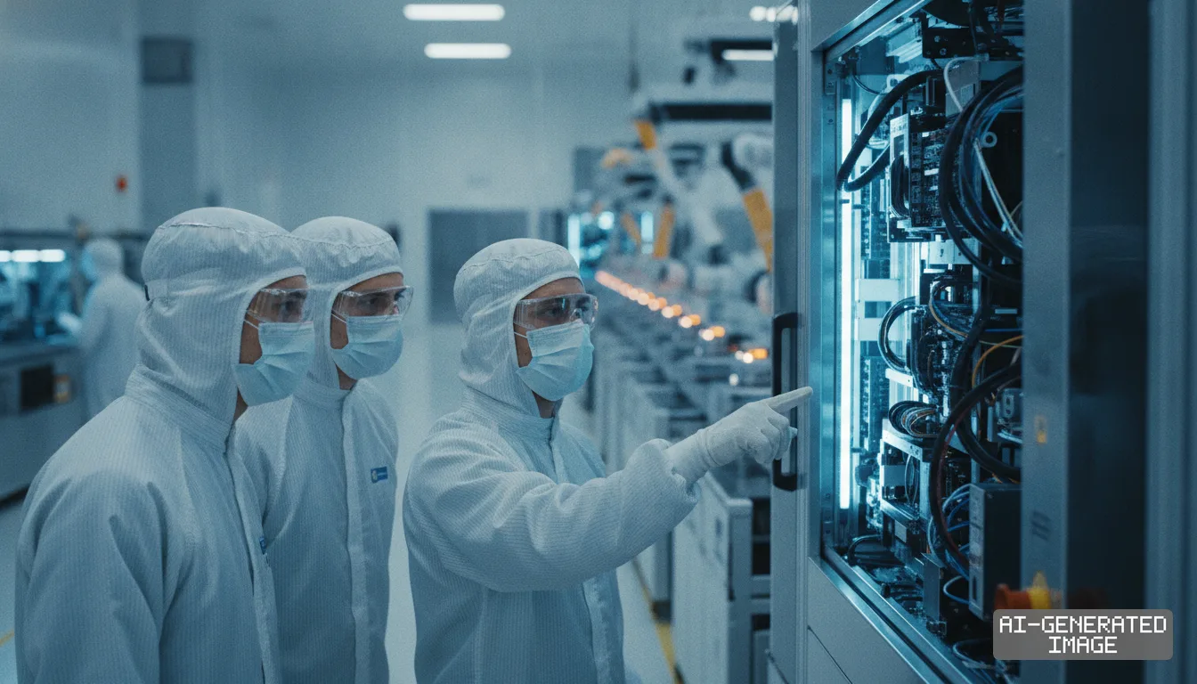
The office sits in the Chiyoda district of Chitose, one block from the local Rapidus office and minutes from the company's IIM-1 wafer fab. The location gives IBM technical staff immediate access to the manufacturing floor.
Japan's Ministry of Economy, Trade and Industry has allocated 2.35 trillion yen ($15.4 billion) in cumulative research subsidies to Rapidus through fiscal 2026. That government funding covers roughly 80% of the startup's total capital commitments to date.
The Chitose base serves as an operational hub for IBM systems engineers working directly on production automation and yield improvement. The team supports fabrication runs and interfaces with municipal authorities and regional suppliers.
Rapidus relies entirely on IBM for its core front-end transistor architecture. The two companies formed a joint development partnership in December 2022 to transfer IBM's 2-nanometer gate-all-around process to Japan.
Gate-all-around — a transistor structure where gate material encloses conductive nanosheet channels on all four sides — allows chips to process data faster while consuming less electrical power. IBM demonstrated the architecture in New York in 2021.
Rapidus dispatched more than 100 engineers to the Albany NanoTech Complex in New York to learn the process. The opening of the Chitose office shifts the center of that engineering work from the United States to Hokkaido.
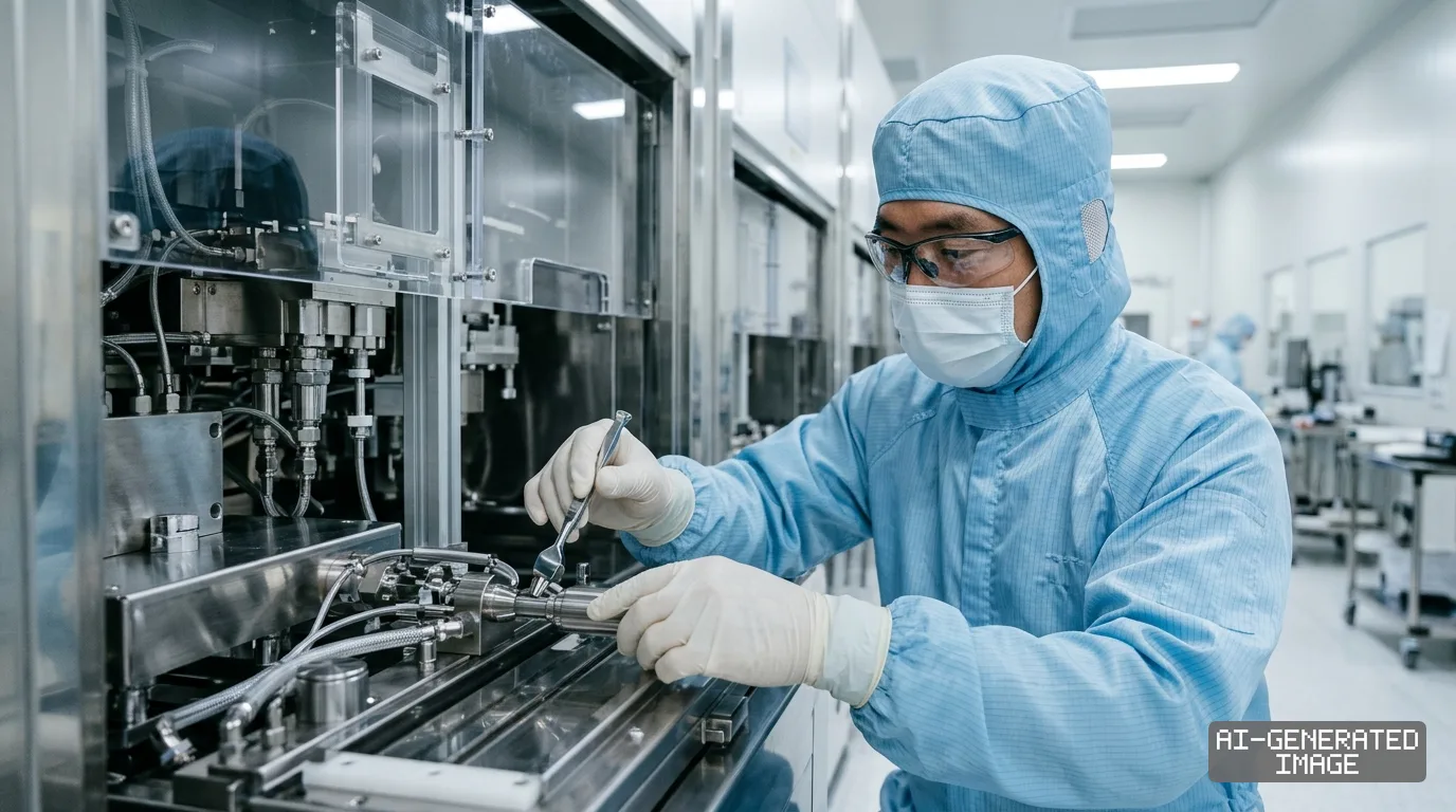
The Chitose site also supports IBM software already integrated into the fab. Rapidus installed IBM's SiView Standard manufacturing execution system — software that tracks materials, directs tooling and manages automated wafer transport — across the IIM-1 line.
The system entered pilot operation in April 2025. It controls wafer movement through extreme ultraviolet lithography equipment installed by ASML, aiming to automate production and reduce turnaround times below those of rival commercial foundries.
Rapidus verified the electrical operation of its first 2-nanometer gate-all-around test transistors at the Chitose plant in July 2025. Engineers are now running test lots to measure defect density and improve baseline production yield.
The venture aims to become Japan's first commercial producer of leading-edge logic below the 28-nanometer node. Domestic Japanese chipmakers exited advanced logic competition more than two decades ago to focus on automotive microcontrollers, power chips and imaging sensors.
Capital requirements remain steep. Rapidus secured 267.6 billion yen ($1.75 billion) in combined public and private equity in February 2026. The Information-technology Promotion Agency provided 100 billion yen, while 32 private companies contributed 167.6 billion yen.
Those private backers include Toyota Motor, Sony Group, SoftBank Corp. and NTT. Despite that equity round, the company still requires an estimated 2 trillion yen in commercial bank loans to build high-volume capacity.
The competitive pressure is intense. Taiwan Semiconductor Manufacturing Co. (TSMC), which holds 62% of the global contract chipmaking market, plans commercial 2-nanometer volume output in late 2025. Samsung Electronics plans to produce its competing SF2 process on a similar timetable.
Both established foundries operate large design ecosystems with hundreds of tape-outs and established customer libraries. Rapidus lacks an established client portfolio and is racing to validate its process design kit with potential customers.
The physical presence of IBM in Chitose is designed to reassure potential fabless clients that the proprietary technology transfer is fully staffed and backed by American research capabilities. The office provides on-site software integration and physical failure analysis.
Rapidus plans to start building a specialized back-end packaging facility at the Chitose site in 2027. That line will assemble advanced multi-die packages using 600-millimeter panel interposers alongside front-end wafer fabrication.
The commercial launch date remains set. Rapidus is targeting mass production of 2-nanometer logic at IIM-1 in the second half of fiscal 2027, beginning with an initial volume of several thousand wafers per month.
The release notice does not state the initial headcount or the capital expenditure allocated to the new Chitose office. IBM Japan has not published hiring targets or long-term staffing figures for the site.
Sources
Primary documents
Reporting
The documents behind this briefing are linked above. East Asia Brief produces its English text with AI assistance under human editorial review, and does not translate or republish other outlets' articles. See our methodology and AI policy. Spotted an error? Tell us.
The Morning Brief
What changed in Korean, Chinese and Japanese industry overnight — and what it means for your supply chain. One email, weekday mornings, US time. Free.
The Morning Brief is in preparation. Leave your address and we will write to you once — when the first issue is ready. Nothing before that.