# SK hynix validates HBM5 with TSMC on next-generation CoWoS
*The South Korean chipmaker secured TSMC's partner award after completing thermal and electrical trials on eighth-generation memory for Nvidia's upcoming Vera Rubin accelerator platform.*
**Published:** September 28, 2026
**By:** Ji-woo Han
**Section:** Semiconductors & AI Hardware — South Korea
**Format:** Breaking
**Confidence:** medium
**Source:** https://eastasiabrief.com/semiconductors/sk-hynix-validates-hbm5-tsmc-next-generation-cowos-415
**Publisher:** East Asia Brief (https://eastasiabrief.com/)
---
## What to know
- SK hynix and TSMC verified HBM5 packaging compatibility on CoWoS lines
- SK hynix commands roughly 60% of global high-bandwidth memory shipments
- JEDEC standardization for eighth-generation HBM specifications remains pending
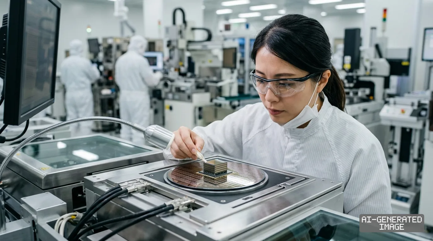
*An engineer inspects a stacked semiconductor chip on a silicon wafer inside an advanced memory packaging cleanroom. (AI-generated image)*
SK hynix announced Sept. 28 it completed joint packaging validation of eighth-generation HBM5 memory with Taiwan Semiconductor Manufacturing Co. at the foundry's annual Open Innovation Platform forum.
The validation took place during technical sessions held Sept. 23 in Santa Clara, California. Both companies are aligning production roadmaps to support Nvidia's upcoming Vera Rubin computing platform.
SK hynix commands roughly 60% of global high-bandwidth memory shipments. The supplier secured TSMC's Partner of the Year award in 3DFabric-HBM integration for the second consecutive year, the company said.
The joint trial evaluated physical, electrical and thermal tolerances of HBM5 memory stacks placed on TSMC's Chip on Wafer on Substrate lines. CoWoS packages combine DRAM stacks directly beside accelerator processors.
Moving to eighth-generation memory requires early design-technology co-optimization between memory makers and foundries. Thermal expansion and mechanical warpage become severe as memory stacks rise to 16 DRAM layers and beyond.
Foundry assembly has emerged as the critical bottleneck in artificial intelligence infrastructure. Delicate high-bandwidth memory dies must withstand the thermal shock and pressure generated by adjacent graphical processing units during heavy workloads.
At the Santa Clara conference, SK hynix displayed a working unit of Nvidia's Vera Rubin superchip. The processor integrates 12-high 36GB HBM4 modules alongside 96GB SOCAMM2 low-power server memory, the company said.
The 12-layer HBM4 configuration transfers high-bandwidth data directly to the Rubin processor core. Meanwhile, the SOCAMM2 module operates as main system memory for the companion Vera central processing unit.
SK hynix also demonstrated high-density memory variations intended for hyperscale cloud data centers. These units featured 16-high 48GB HBM4 stacks as well as 12-high 48GB HBM4E engineering samples.
The South Korean memory producer began commercial shipments of sixth-generation HBM4 in the second quarter of 2026. Customer sampling for seventh-generation HBM4E units is currently underway, according to company releases.
To support broader data center clusters, SK hynix showcased enterprise server modules alongside high-bandwidth stacks. Displays included a 256GB registered dual in-line memory module, the largest capacity currently available in commercial production.
The exhibit also featured 128GB multiplexer combined RDIMMs and 64GB RDIMMs fabricated on sixth-generation 10-nanometer-class nodes. High-density server DRAM helps reduce data transfer bottlenecks during large-scale model training.
In enterprise storage, SK hynix introduced solid-state drives engineered for liquid-cooled server racks. Its PEB210 drive supports direct liquid cooling configurations to improve power efficiency in enterprise installations.
A companion PS1101 storage drive uses quad-level cell NAND flash to lower power consumption in cloud facilities. SK hynix also presented a development roadmap for PCIe Gen 6 and Gen 7 chiplet storage interfaces.
Nvidia represents the primary destination for these advanced memory architectures. The American chip designer holds more than 70% of global AI accelerator revenue and relies on TSMC for logic fabrication and packaging.
Rival memory suppliers are pursuing identical packaging certifications with the Taiwanese foundry. Micron Technology accounts for about 20% of the high-bandwidth memory market and is ramping HBM4 production for Nvidia hardware.
Samsung Electronics controls roughly 15% of high-bandwidth memory shipments worldwide. Samsung operates its own turnkey packaging lines while simultaneously qualifying memory stacks for integration with TSMC's external CoWoS production flow.
Industry engineering reports show TSMC is running parallel thermal and mechanical stress tests on HBM5 with Samsung and Micron. Foundry engineers must evaluate mechanical warpage across diverse silicon base die structures.
Custom base dies mark a major structural transition in the semiconductor supply chain. Prior high-bandwidth memory generations relied on conventional DRAM production lines to fabricate the underlying logic control die.
Starting with HBM4 and continuing into HBM5, base dies are manufactured on advanced logic foundry processes. Foundries etch custom routing channels and test circuits directly into the base wafer, the company said.
This architectural change ties memory manufacturers directly to TSMC's advanced logic capacity. Memory vendors can no longer build high-end memory stacks without accessing precision lithography from external contract foundries.
Packaging yields on TSMC's CoWoS lines will govern delivery schedules for next-generation computing hardware. A single microscopic flaw in the base die or micro-bump array ruins the entire multi-chip module.
The notice does not state whether the validated HBM5 stack uses a 4,096-bit interface bus or full copper-to-copper hybrid bonding. Those structural parameters await formal publication by the JEDEC Solid State Technology Association.
TSMC and SK hynix also did not disclose electrical test yields, thermal dissipation metrics, or sampling schedules for the validated test vehicles. Both companies treat early testing data as confidential proprietary property.
JEDEC standards committees are scheduled to review preliminary HBM5 specification drafts in December 2026. Commercial volume manufacturing of eighth-generation memory stacks is scheduled to follow Rubin hardware rollouts across 2027.
## Impact map
| Event | Korea | China | Japan | Global impact |
| --- | --- | --- | --- | --- |
| HBM5 packaging validation | SK hynix defends ~60% HBM share, Samsung qualifies secondary CoWoS flow | Domestic accelerator developers face expanding memory gap without 2.5D packaging access | Packaging tool builders Tokyo Electron and Disco see CoWoS demand stretch into 2027 | Nvidia solidifies high-bandwidth memory supply for Vera Rubin data center deployments |
## In this story
- **Companies:** SK hynix, TSMC, Nvidia
- **Tickers:** 000660.KS, 2330.TW, NVDA
- **Exposed:** Samsung Electronics, Micron Technology
- **Policy:** Economic Security
- **Impact:** Supply Chain, Capex, Packaging
## Primary sources
1. skhynix.co.kr
2. daum.net
3. industrynews.co.kr
4. financialpost.co.kr
5. newstomato.com
---
Cite as: East Asia Brief, "SK hynix validates HBM5 with TSMC on next-generation CoWoS," September 28, 2026. https://eastasiabrief.com/semiconductors/sk-hynix-validates-hbm5-tsmc-next-generation-cowos-415