# Kioxia and Sandisk split roadmaps for 3D NAND hybrid bonding in Japan
*The joint venture partners diverge on equipment choices at their shared manufacturing base even as they commit $31 billion to memory capacity through 2032.*
**Published:** November 4, 2026
**By:** Kenji Sato
**Section:** Semiconductors & AI Hardware — Japan
**Format:** Why It Matters
**Confidence:** medium
**Source:** https://eastasiabrief.com/semiconductors/kioxia-sandisk-split-roadmaps-3d-nand-hybrid-bonding-japan-1114
**Publisher:** East Asia Brief (https://eastasiabrief.com/)
---
## What to know
- Kioxia and Sandisk diverge on hybrid bonding roadmaps at their shared Yokkaichi fab complex
- Sandisk owes $1.165 billion in joint venture cash payments to Kioxia across 2026 to 2029
- The alliance reviews annual tool allocation budgets before the Japanese fiscal year closes in March 2027
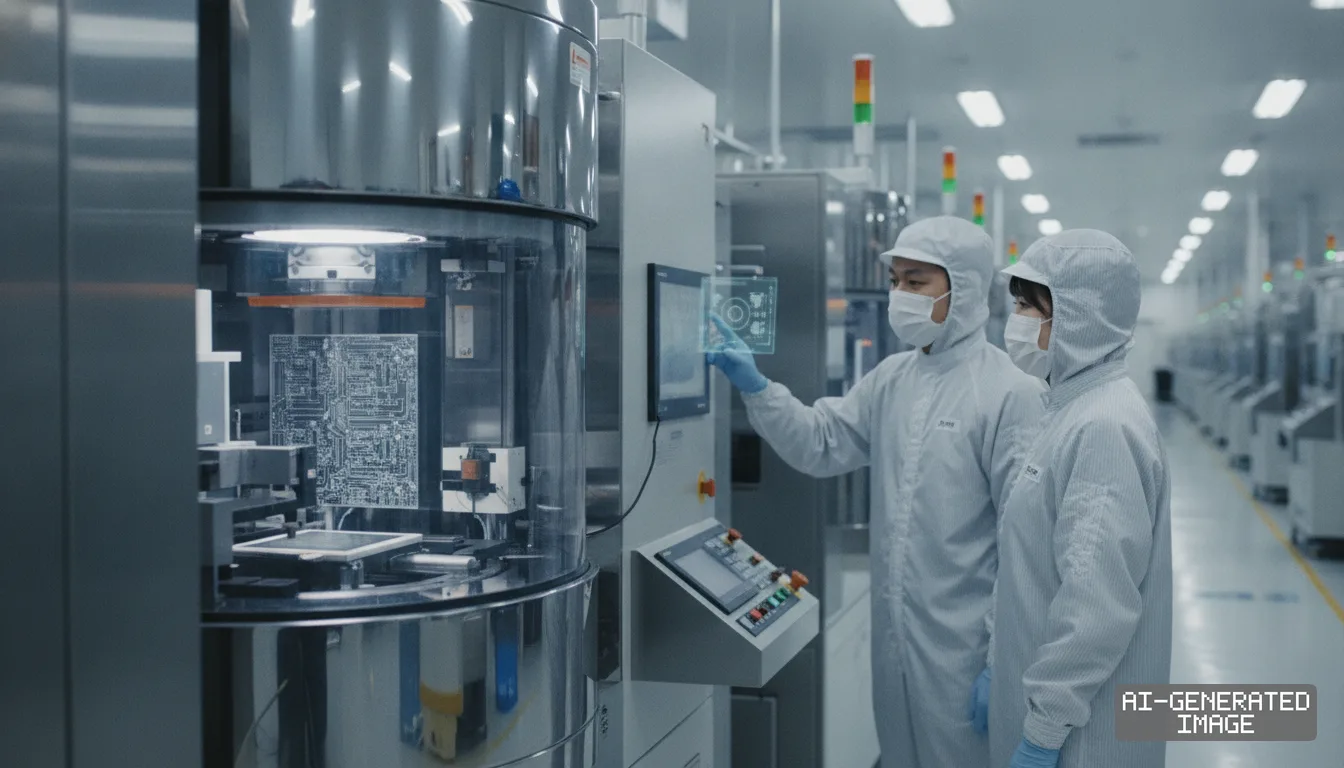
*Technicians in cleanroom suits operate semiconductor manufacturing equipment on an advanced memory chip production line. (AI-generated image)*
Kioxia Holdings and Sandisk Corporation moved toward diverging manufacturing roadmaps for 3D NAND hybrid bonding at their joint Yokkaichi complex on Nov. 3, 2026, splitting their equipment requirements for ultra-high-density storage chips.
The Yokkaichi plant in Mie Prefecture operates as the world's largest NAND flash manufacturing site. The complex processes roughly 250,000 wafer starts monthly, accounting for nearly 30% of global flash memory production.
Under the joint venture agreement, Kioxia controls 60% of total production volume across Yokkaichi and Kitakami, while Sandisk takes 40%. The partners committed over $31 billion in combined capital spending through 2032.
Hybrid bonding — a technique joining two polished silicon wafers directly using copper pads without intervening microbumps — has become essential for flash chips exceeding 300 vertical layers. The architecture separates logic from memory arrays.
The partners introduced wafer-to-wafer direct bonding in their eighth-generation BiCS8 architecture, which stacks 218 cell layers. They named the design CMOS directly Bonded to Array, or CBA, to lower thermal stress on CMOS circuits.
In standard CBA fabrication, workers produce peripheral CMOS circuitry on one silicon substrate and build the storage array on another. Cleanroom tools then bond the two finished wafers face-to-face under deep vacuum conditions.
Technical divergence emerged as each company evaluated next-generation architectures designed to scale beyond 1,000 word lines. Kioxia developed a multi-stacked approach requiring multiple consecutive wafer bonds, while Sandisk favored retaining single-step bonding to control tooling costs.
Kioxia demonstrated a multi-stacked CBA architecture using wafer-to-wafer copper bonding on Oct. 27, 2026. The prototype proved functional four-bit quad-level cell operation across stacked memory arrays, the company said in an engineering report.
The multi-stack process requires stacking two or more memory cell array wafers atop a single CMOS control wafer. That structure increases storage capacity per chip but multiplies the number of chemical-mechanical planarization and bonding steps.
Sandisk prioritized capital discipline following its spin-off from Western Digital. The company told investors in August that it targets bit growth through process refinement rather than raw cleanroom expansion, aiming to lower capital spending as a share of revenue.
Operating divergent process flows inside a shared manufacturing complex alters operational economics. The joint venture leases equipment to Kioxia, which manages daily fab operations and bills manufacturing costs back to Sandisk based on capacity share.
Separate process routes require dedicated wafer bonders and bespoke surface preparation chambers. Installing parallel tool sets reduces the procurement discounts that Kioxia and Sandisk achieved when ordering identical lines for past BiCS generations.
The divergence alters supply schedules for advanced packaging and metrology equipment. Kioxia co-developed specialized infrared inspection tools with KLA Corporation to measure bonding overlay accuracy before silicon thinning, according to technical documents published by the company.
Global flash makers are shifting to hybrid bonding to bypass physical limits of etching deep memory holes. Samsung Electronics holds 31% of worldwide NAND capacity and SK hynix holds 20%, both developing proprietary wafer-bonding flows.
Public subsidies underpin ongoing cleanroom construction across both partner sites in Japan. Japan's Ministry of Economy, Trade and Industry approved up to ¥243 billion ($1.6 billion) in grants to support advanced memory production at Yokkaichi and Kitakami.
The companies extended their foundational joint venture framework through Dec. 31, 2034, in January 2026. Under that agreement, Sandisk agreed to pay Kioxia $1.165 billion in cash installments between 2026 and 2029 for manufacturing services.
Kioxia issued conservative operating profit projections for the fourth quarter on Oct. 30, 2026, citing cautious enterprise procurement. Shares of Sandisk rose 6.5% on the Nasdaq following the earnings update.
Sandisk makes its next scheduled cash installment of the $1.165 billion manufacturing agreement in December 2026. The joint operating committee conducts its formal tool allocation review before the close of the Japanese fiscal year in March 2027.
Neither Kioxia Holdings nor Sandisk Corporation published regulatory filings or formal company statements on Nov. 3 detailing specific tool contracts or permanent process separations for the Yokkaichi complex.
Both memory makers continue active volume manufacturing of 218-layer BiCS8 flash chips on shared fabrication lines across six operational cleanrooms at the Mie Prefecture site.
## Impact map
| Event | Korea | China | Japan | Global impact |
| --- | --- | --- | --- | --- |
| Hybrid bonding roadmap divergence | Samsung and SK hynix retain single-line bonding efficiency across 51% of global NAND output | YMTC faces widening tool access gap under western export controls | Kioxia manages higher cleanroom tool complexity across 60% of Yokkaichi capacity | Flash buyers face bifurcated high-layer SSD component qualification schedules |
| Hybrid bonding roadmap divergence | Samsung and SK hynix retain single-line bonding efficiency across 51% of global NAND output | YMTC faces widening tool access gap under western export controls | Kioxia manages higher cleanroom tool complexity across 60% of Yokkaichi capacity | Flash buyers face bifurcated high-layer SSD component qualification schedules |
## In this story
- **Companies:** Kioxia Holdings, Sandisk Corporation
- **Tickers:** 285A.T, SNDK
- **Exposed:** KLA Corporation, Samsung Electronics, SK hynix
- **Policy:** Subsidies
- **Impact:** Capex, Supply Chain, Cost Structure
## Primary sources
1. chosun.com
2. kioxia.com
3. tomshardware.com
4. sandisk.com
5. fool.com
---
Cite as: East Asia Brief, "Kioxia and Sandisk split roadmaps for 3D NAND hybrid bonding in Japan," November 4, 2026. https://eastasiabrief.com/semiconductors/kioxia-sandisk-split-roadmaps-3d-nand-hybrid-bonding-japan-1114