# Google turns to Samsung and SK hynix HBM as custom TPU fleet grows
*Alphabet will absorb 36% of worldwide high-bandwidth memory demand by 2027, trailing Nvidia by just 1.3 percentage points on custom accelerator demand.*
**Published:** November 12, 2026
**By:** Ji-woo Han
**Section:** Semiconductors & AI Hardware — South Korea
**Format:** Why It Matters
**Confidence:** medium
**Source:** https://eastasiabrief.com/semiconductors/google-turns-samsung-sk-hynix-hbm-custom-tpu-fleet-1347
**Publisher:** East Asia Brief (https://eastasiabrief.com/)
---
## What to know
- Google expands TPU 8th-gen family to four systems, lifting TPU 8i Max HBM capacity to 384GB
- Morgan Stanley estimates Google will account for 36.0% of global HBM demand by 2027 vs Nvidia at 37.3%
- Google plans commercial deployment of TPU 8tx and TPU 8i Max hardware in early 2027
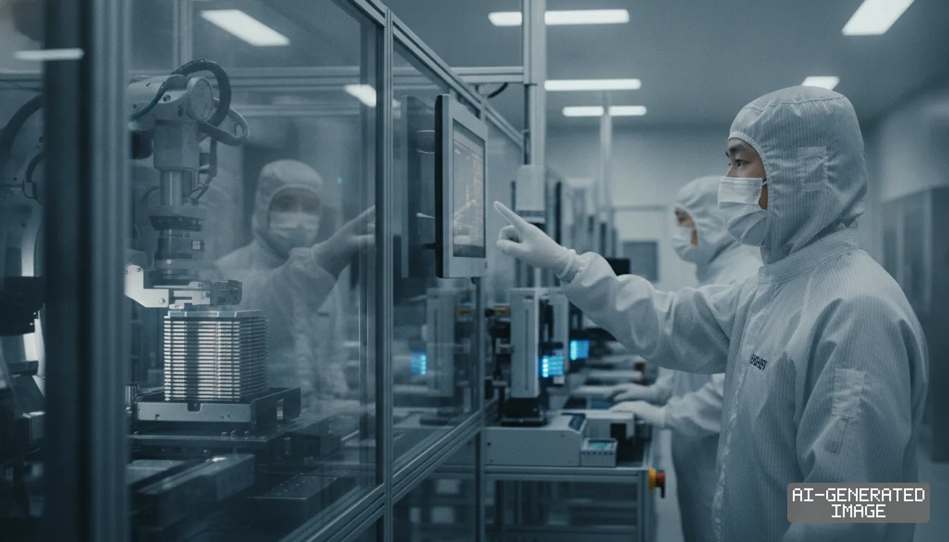
*Technicians in cleanroom suits monitor automated robotic machinery handling stacked semiconductor chips along a production line. (AI-generated image)*
Google expanded its custom artificial intelligence silicon pipeline on Nov. 11, creating a direct pathway for Samsung Electronics and SK hynix to widen high-bandwidth memory supply deals beyond graphics processor orders.
The expansion reshapes global memory procurement as custom accelerators challenge merchant graphics processors. Morgan Stanley projects Google will absorb 36.0% of worldwide high-bandwidth memory demand by 2027, trailing Nvidia's 37.3% share by 1.3 percentage points.
High-bandwidth memory (HBM) — stacks of dynamic random-access memory dies connected by microscopic vertical wires — eliminates latency bottlenecks in high-density computing clusters. Memory makers package these stacks directly beside processor dies.
Google Cloud generated $30.71 billion in revenue during the third quarter of 2026. Growing cloud operations support nearly 100 enterprise accelerator customers, including artificial intelligence research lab Anthropic, accelerating internal chip deployments.
The expanded hardware strategy relies on Google's eighth-generation Tensor Processing Unit family. Google completed the four-processor lineup on Nov. 9 by unveiling the TPU 8tx and TPU 8i Max systems for enterprise workloads.
System-level integration allows engineers to reconfigure compute, memory and networking around proven silicon within months, Amin Vahdat, Google's chief technologist for AI and infrastructure, said in the product announcement.
The dual-chip TPU 8i Max integrates two inference dies into a single package. The hardware combines 384 gigabytes of high-bandwidth memory and delivers 17.2 terabytes per second of memory bandwidth across operations.
That configuration doubles compute throughput and provides 768 megabytes of on-chip static random-access memory. Google designed the dual-chip assembly to process massive reasoning context windows within existing data center server racks.
The new systems join two base processors released in April. Google launched the training-oriented TPU 8t with 216 gigabytes of HBM and the inference-focused TPU 8i with 288 gigabytes of fifth-generation memory stacks.
Google also introduced the TPU 8tx system for confidential artificial intelligence execution. The system connects training-grade silicon to fifth-generation AMD EPYC host processors, maintaining cryptographic hardware isolation during enterprise fine-tuning and inference tasks.
Software additions accompany the hardware rollout to ease customer adoption. Google open-sourced TorchTPU for native framework execution and launched specialized networking utilities to reduce data transfer latency across large accelerator clusters.
The widening accelerator slate alters commercial dynamics for South Korean memory manufacturers. Samsung Electronics and SK hynix previously allocated the vast majority of their high-bandwidth memory capacity to single-buyer graphics processor supply chains.
SK hynix moved to align its engineering roadmaps with Alphabet earlier in the year. SK Group Chairman Chey Tae-won met Google Chief Executive Officer Sundar Pichai on Feb. 13 to pursue custom HBM co-design.
Customized memory stacks require tight architectural integration between the memory base die and host silicon. Joint design initiatives allow SK hynix to lock in multiyear volume commitments ahead of major generational transitions.
Samsung Electronics is broadening its custom silicon footprint through Google's primary design partner, Broadcom. Broadcom designs the core application-specific integrated circuit architecture used in Google's highest-performance tensor processing units.
The partnership allows Samsung Electronics to supply high-bandwidth memory alongside advanced 2.5-dimensional packaging services. Combining memory manufacturing with packaging integration positions the company to secure turnkey contracts from cloud service providers.
Hyperscalers are expanding proprietary chip programs to control operating expenses. Purpose-built application-specific integrated circuits cut computing costs by roughly 30% compared to standard merchant graphics processing units, while optimizing server thermal profiles.
Tailored silicon architectures shift hardware expenditure from general-purpose computing logic toward memory capacity. High-capacity accelerators like the TPU 8i Max require up to 384 gigabytes of memory, driving higher silicon content per board.
Diversifying memory supply chains reduces Korean manufacturers' reliance on merchant GPU release schedules. Serving multiple hyperscaler custom silicon programs shields component makers from inventory adjustments and single-customer negotiating leverage.
Production bottlenecks still constrain the pace of deployment across the semiconductor sector. Advanced packaging facilities and high-precision through-silicon via lines remain fully booked across global assembly contractors through late 2027.
Google's product notice did not state vendor allocation percentages, contract values or unit pricing for memory purchased from Samsung Electronics and SK hynix, keeping commercial supply terms undisclosed.
Google scheduled external commercial deployment of the TPU 8tx and TPU 8i Max systems for early 2027. Next-generation two-nanometer tensor processing unit hardware remains scheduled to enter volume manufacturing in mid-2028.
## Impact map
| Event | Korea | China | Japan | Global impact |
| --- | --- | --- | --- | --- |
| Custom ASIC HBM diversification | Samsung and SK hynix capture custom TPU orders, diluting single-buyer GPU concentration | cloud providers face restricted access to equivalent high-density accelerator memory | semiconductor packaging and substrate vendors receive expanded multi-die orders | Google closes HBM consumption gap with Nvidia to 1.3 percentage points by 2027 |
## In this story
- **Companies:** Alphabet, Samsung Electronics, SK hynix
- **Tickers:** 005930.KS, 000660.KS
- **Exposed:** Broadcom, Advanced Micro Devices, Nvidia
- **Impact:** Supply Chain, Order Book, Capex
## Primary sources
1. blog.google
2. edaily.co.kr
3. jabon.co.kr
4. trendforce.com
5. vlsi.kr
---
Cite as: East Asia Brief, "Google turns to Samsung and SK hynix HBM as custom TPU fleet grows," November 12, 2026. https://eastasiabrief.com/semiconductors/google-turns-samsung-sk-hynix-hbm-custom-tpu-fleet-1347